
Eureka
For R&D, Eureka makes reading and utilizing patents & technical documents easy.
Eureka AIR
Designed for self-driven R&D workflows. Generate viable solutions, solve complex R&D challenges, empower your innovation with AI.

Eureka Materials
Designed for material experts only. Revolutionize your material R&D, from search, analyze, to developing new materials.

TechResearch
Generate reliable direction feasibility study reports for your R&D in just a few steps.

TechSeek
Discover and master advanced knowledge NOW. Basics, ideas, possibilities, all at once.

TechMind
As an expert in R&D Theories, TechMind can generates customized viable solutions instantly.

TechRisk
Analyze your overall solution with one click, know your potential R&D risks in advance.

TechMonitor
Get weekly tech updates, stay abreast of the latest tech innovations and key insights.
SCALABLE CIRCUIT-UNDER-PAD DEVICE TOPOLOGIES FOR LATERAL GaN POWER TRANSISTORS
- Summary
- Abstract
- Description
- Claims
- Application Information
AI Technical Summary
Benefits of technology
Problems solved by technology
Method used
Image

Examples
first embodiment
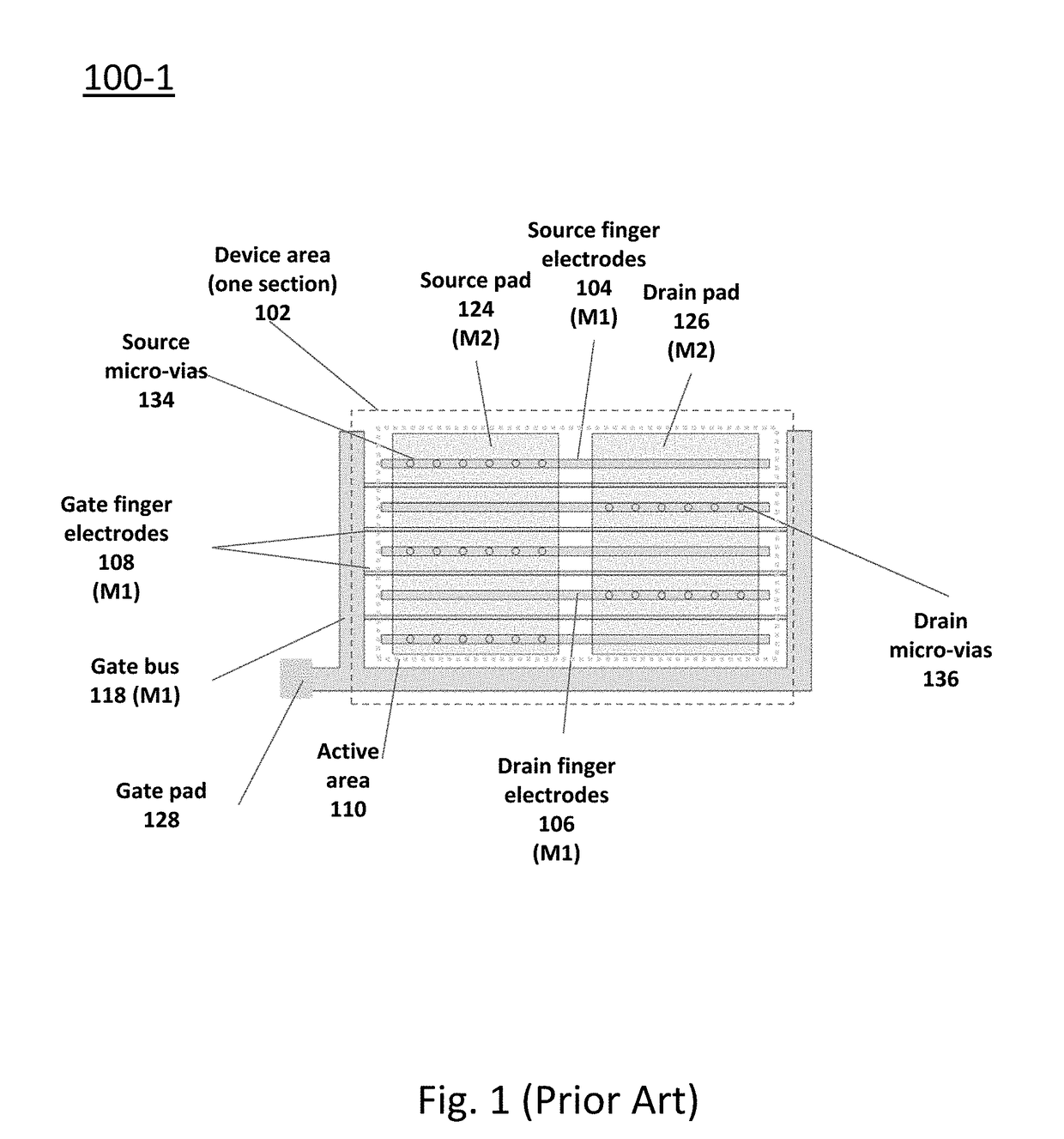
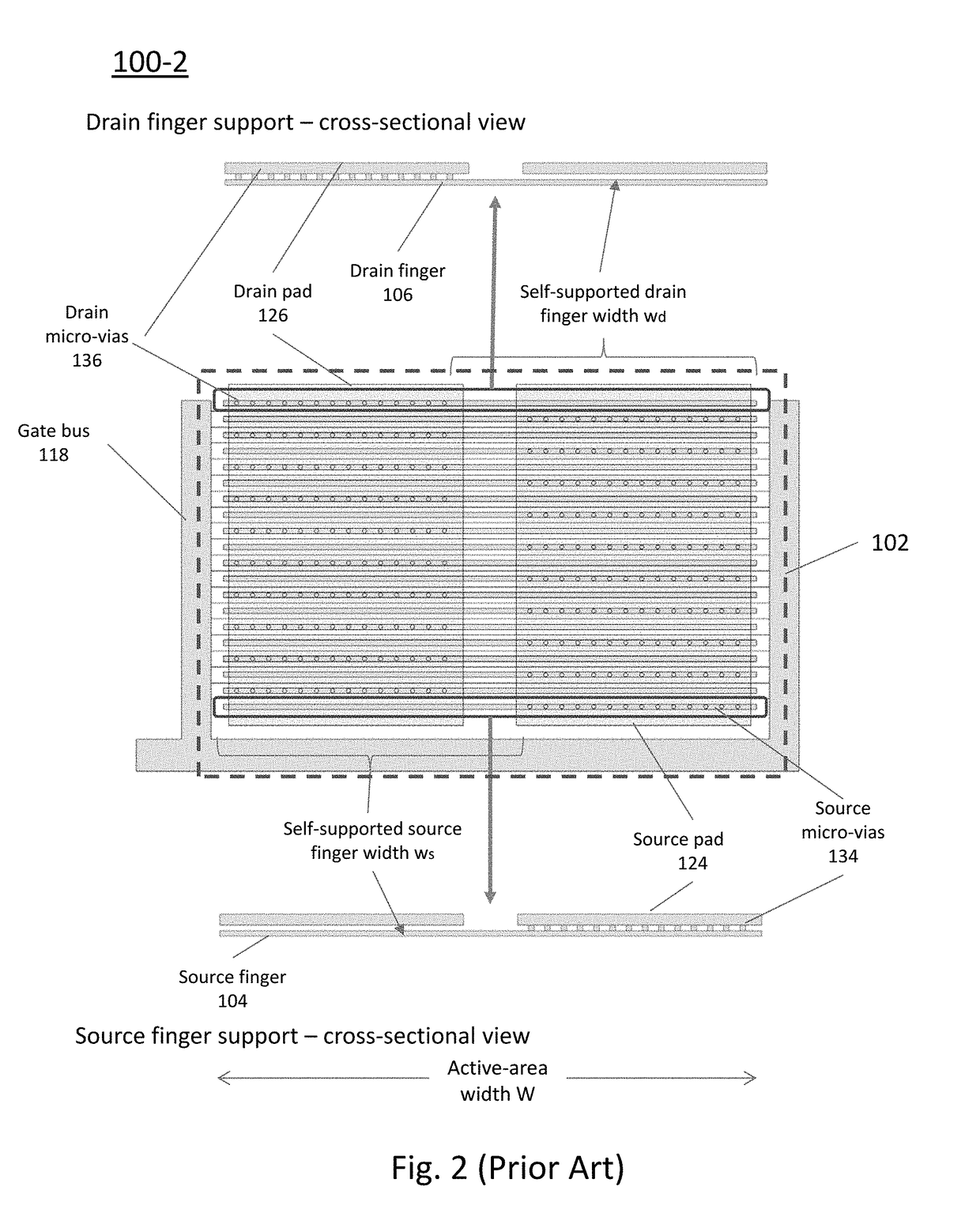
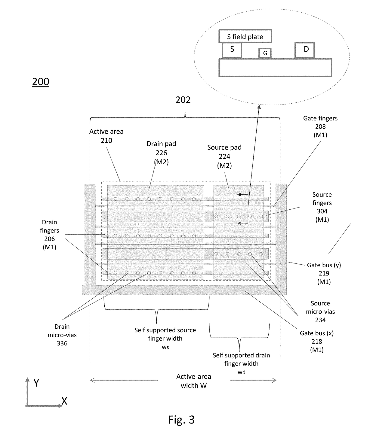
[0057]FIG. 4. shows a schematic diagram of a top plan view of part of a GaN die in the form of a GaN-on-silicon device structure 300 comprising one section 302 of a lateral GaN transistor arranged as a multi-section transistor according to a For example, the lateral GaN transistor structure comprises a GaN epitaxial layer stack formed on a silicon substrate, and the epitaxial layer stack comprises GaN / AlGaN heterostructure layers which define an active area, i.e. a 2 DEG active region 310 for each transistor section 302. A first metallization layer M1 is patterned to form an array of source finger electrodes 304 and drain finger electrodes 306 on each active region 310 of the substrate. The first metallization layer also defines gate finger electrodes 308 running between source fingers 304 and drain fingers 306, and a gate bus having a first portion 318 running in an x direction over an inactive region along one edge of the active area, and second portions 319 running in a y direct...
second embodiment
[0062]FIG. 6A shows a schematic diagram of a top plan view of a GaN-on-silicon device structure 500A comprising one section of a multi-section lateral GaN transistor to illustrate patterning of first and second metallization layers M1 and M2. Many elements of this device structure are similar to those shown in FIG. 5 and are numbered with the same reference numerals incremented by 100. This variant of the three-piece pad device topology differs from that shown in FIG. 4 in that the first and second source pads 524 are separated from the source pads of adjacent sections, and only partly overlap the adjacent underlying second portion of the gate buses 519. In another variant of the device structure 500B, as shown in FIG. 6B, the source pads 524 may be defined only over the active area, without overlapping the adjacent second portions of the gate buses 519. Source pads 524 are spaced from source pads of neighbouring sections. In contrast, as illustrated in FIG. 4, the source pads 424 ...
fourth embodiment
[0063]FIG. 7 shows a schematic diagram of a top plan view of a GaN-on-silicon device structure 600 comprising one cell or section 602 of a multi-section lateral GaN transistor of a fourth embodiment, to illustrate patterning of a first and second conductive metallization layers M1 and M2. The first level of metallization M1 is patterned to define source, drain and gate fingers on active areas of each section, and gate buses as for the device structures of the embodiments described above. In the device structure 600 of this embodiment, each section comprises a three-piece pad structure, similar to those shown in FIGS. 5, 6A and 6B. However adjacent edges of the source pads 624 and drain pads 626 comprise “castellations”644 and 646 respectively. For example, as illustrated schematically, the edges of the source and drain pads are notched or crenellated to form rectangular castellations. The source castellations 644 extend from the main part of the source pad 624 and source micro-vias ...
PUM
 Abstract
Description
Claims
Application Information
 - R&D Engineer
- R&D Manager
- IP Professional
- Industry Leading Data Capabilities
- Powerful AI technology
- Patent DNA Extraction
Browse by: Latest US Patents, China's latest patents, Technical Efficacy Thesaurus, Application Domain, Technology Topic, Popular Technical Reports.
© 2024 PatSnap. All rights reserved.Legal|Privacy policy|Modern Slavery Act Transparency Statement|Sitemap|About US| Contact US: help@patsnap.com