Device modifying the impedance value of a reference resistor

a reference resistor and device technology, applied in the direction of network simulating resistances, electrical apparatus, electronic switching, etc., can solve the problems of stray, parasitic, stray, etc., and the device is not adapted to form hvr resistors,

Active Publication Date: 2019-03-14
COMMISSARIAT A LENERGIE ATOMIQUE ET AUX ENERGIES ALTERNATIVES
View PDF3 Cites 2 Cited by
  • Summary
  • Abstract
  • Description
  • Claims
  • Application Information

AI Technical Summary

Benefits of technology

[0050]The device may further include at least two resistors forming a voltage dividing bridge, the reference resistor being connected, or coupled, in parallel to one of the two resistors of the voltage dividing b

Problems solved by technology

However, these devices are not adapted to form HVR resistors because of their too high switching noise.
Each of these solutions however has at least one of the following drawbacks: the voltage dynamics is too low (a few tens of mV at best), the equivalent noise is too high, the stray, or parasitic, capacitance is t

Method used


Image

  • Device modifying the impedance value of a reference resistor
  • Device modifying the impedance value of a reference resistor
  • Device modifying the impedance value of a reference resistor

Examples


first embodiment

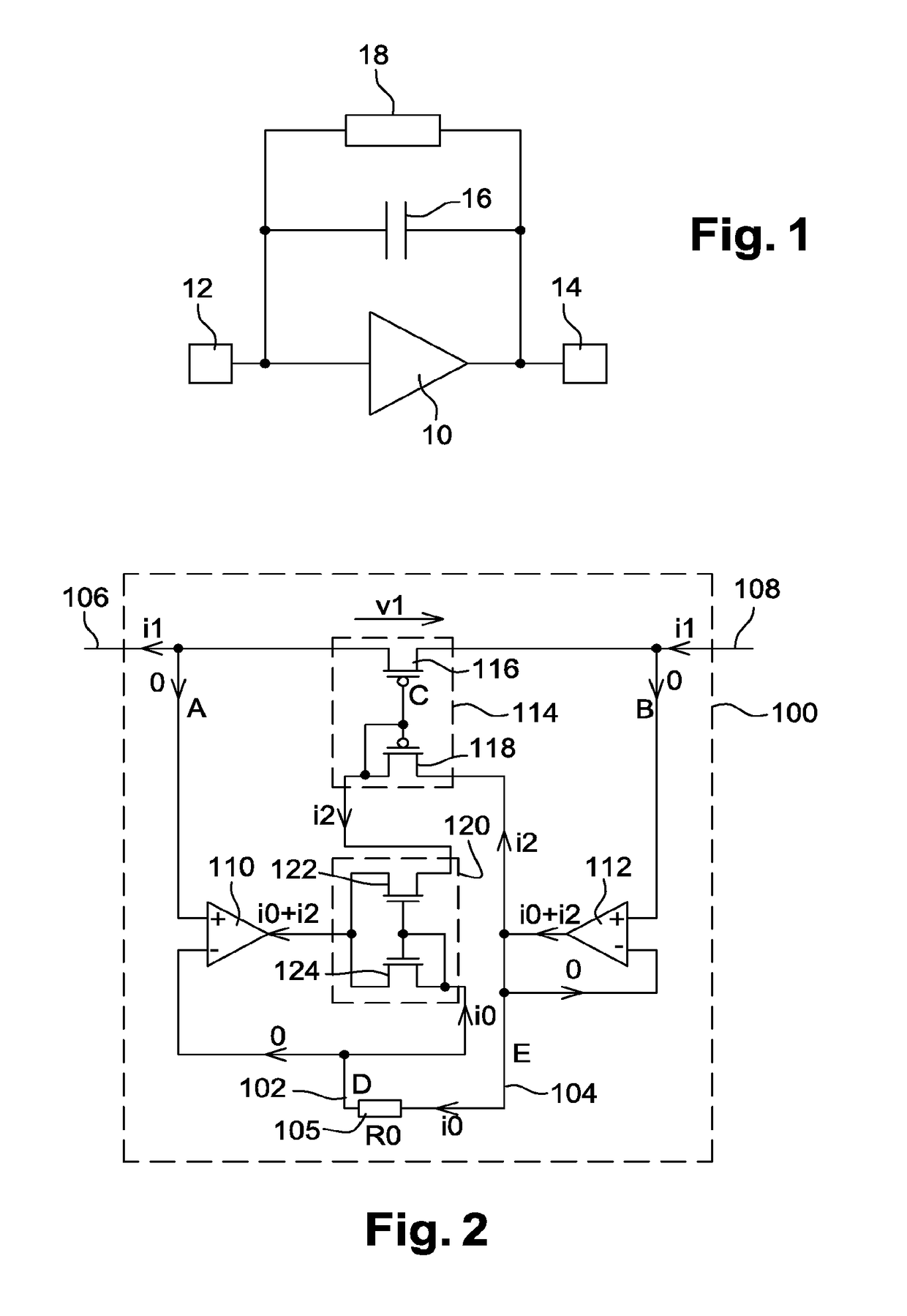
[0072]FIG. 2 shows an electronic device 100 enabling the impedance value of a reference resistor 105 to be modified.

[0073]The device 100 includes two first terminals 102, 104 to which the reference resistor 105 is connected. An electric potential VD is intended to be obtained on the terminal 102 and an electric potential VE is intended to be obtained on the terminal 104. The reference resistor 105 has an impedance with the value R0 and is such that a current i0 passes therethrough because of a voltage VDE applied between both first terminals 102, 104 and to which the reference resistor 105 is subjected.

[0074]The device 100 also includes two second terminals 106, 108 between which a modified impedance value of the reference resistor 105 is intended to be obtained. An electric potential VA is intended to be obtained on the terminal 106 and an electric potential VB is intended to be obtained on the terminal 108. The device 100 is such that a current i1 passes therethrough, via the sec...

second embodiment

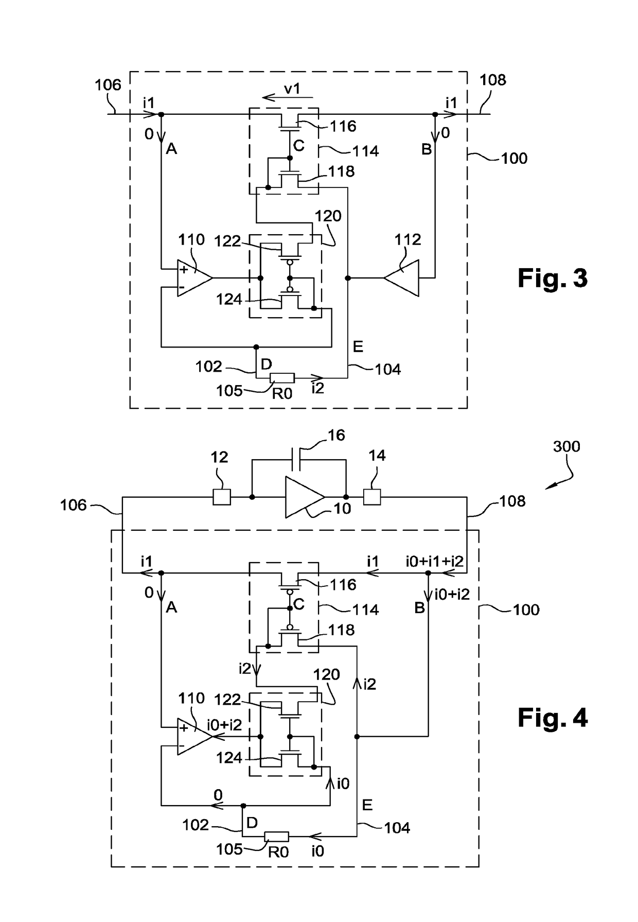
[0092]FIG. 3 shows a device 100 for modifying an impedance according to a

[0093]The device 100 according to this second embodiment includes the same elements as those of the device 100 according to the first embodiment shown in FIG. 2, that is the operational amplifiers 110, 112 (in FIG. 3, a single input of the amplifier 112 which is connected as a follower is shown, this single input corresponding to the non-inverting input of the operational amplifier 112) and the current mirrors 114, 120 formed by the FET transistors 116, 118, 122 and 124. Unlike the first embodiment, the FET transistors 116, 118 are here of the N type and the FET transistors 122, 124 are of the P type. By thus inverting the polarity of the FET transistors, the device 100 shown in FIG. 3 is adapted to operate with VBA. The operation of this device 100 is analogous to that previously described in connection with FIG. 2.

[0094]According to another embodiment, in order to have a device for modifying the impedance val...

third embodiment

[0096]In some cases, for example if the device 100 is feedback connected to a charge amplifier, the low-impedance output of the charge amplifier is thereby able to provide the current i0+i2 required for operating the device 100. In this case, the device 100 may not include the operational amplifier 112, with therefore the reference resistor 105 directly connected to the drains of the FET transistors 116, 118 of the first current mirror 114. FIG. 4 shows an electronic circuit 300 including the device 100 which corresponds to the configuration described above, that is feedback connected to the charge amplifier 10 (here in a configuration similar to that of that previously described in connection with FIG. 1). The terminal 104 is directly connected to the drains of the FET transistors 116, 118 of the first current mirror 114 as well as to the terminal 108.

[0097]Further, in the configuration shown in FIG. 4, the electric potentials VB and VA are permanently such that VB>VA. Thus, addin...


PUM


Abstract

An electronic device including at least:
    • a reference resistor;
    • two first terminals between which the reference resistor is connected, and two second terminals between which a modified impedance value of the reference resistor is intended to be obtained;
    • a first circuit configured to apply between the two second terminals a voltage substantially equal to that between the two first terminals;
    • a second circuit configured to flow between the two second terminals a second current the value of which corresponds to a fraction of a first current for flowing in the reference resistor between the two first terminals.

Description

TECHNICAL FIELD AND PRIOR ART[0001]The invention relates to a device modifying the impedance value of a reference resistor and outputting this modified impedance value. The invention is advantageously used to form a high value resistor (HVR) the impedance of which is for example higher than or equal to about 1 MΩ.[0002]In the field of microelectronics, it is sometimes necessary to have a continuous time HVR. This is the case with a charge amplifier used for example in spectrometry to detect the electric signals created by the impact of photons in the detector. Such a charge amplifier 10 is shown in FIG. 1. The charge amplifier 10 includes an input 12 and an output 14 to which an integration capacitance 16 and an HVR 18, in parallel to the charge amplifier 10, are connected. The impedance value of the HVR 18 is for example in the order of 1 GΩ and that of the integration capacitance 16 in the order of a few tens of femtofarads (fF). The HVR 18 must have a low value stray capacitance ...

Claims


Application Information

Patent Timeline
IPC IPC(8): H03K17/687H03F3/70H03F3/45
CPCH03K17/687H03F3/70H03F3/45179H03F2200/129H03F2200/144H03H11/53
Inventor ROSTAING, JEAN-PIERREPEIZERAT, ARNAUD
Owner COMMISSARIAT A LENERGIE ATOMIQUE ET AUX ENERGIES ALTERNATIVES
Why Eureka
Try Eureka