Method for manufacturing electronic products, related arrangement and product

a technology of electronic products and related arrangements, applied in the direction of dielectric characteristics, dielectric pattern formation, dielectric association of printed circuit non-printed electric components, etc., can solve the problems of insufficient economic and reliable, large amount of components cannot be printed, solder paste and conductive adhesive based solutions have turned out to be problematic, etc., to achieve simple, short and cost-efficient overall process, reduce and the effect of reducing the number of manufacturing steps

Inactive Publication Date: 2019-03-21
TACTOTEK
View PDF9 Cites 0 Cited by
  • Summary
  • Abstract
  • Description
  • Claims
  • Application Information

AI Technical Summary

Benefits of technology

[0031]The utility of the embodiments of the present invention results from a variety of different issues. The suggested method involves a reduced number of manufacturing steps relative to many prior art alternatives due to the use of conductive ink for establishing both conductor traces and contact pads for the components, thus yielding simple, short and cost-efficient overall process. The conductive ink, which is preferably substantially nonadhesive, tolerates stretching, bending, shaking, etc. better than at least most of the conductive adhesives, and has better conductivity as well.
[0032]The substrate and other elements are also typically subjected to lower thermal stress than in conjunction with solder-based arrangements, which preserves their advantageous properties and reduces heat-generated artifacts.
[0034]Potentially rather considerable physical fixing characteristics provided by some conventional conductive adhesives are not required in the context of the present invention as fully satisfactory physical attachment may be obtained by utilizing e.g. the combination of traditional non-conductive adhesive, such as epoxy, and e.g. molded plastics to secure the component, such as package or body, to the substrate. Also the (wet) ink may be selected so as to facilitate retaining the component(s) in place at least temporarily prior to subsequent process steps such as heating and / or moulding steps.
[0035]The obtained optical quality of the manufactured device or generally product is high as deteriorations caused by aggressive, penetrative and often colored, conductive adhesives are omitted through use of more passive conductive ink(s) and potential non-conductive, merely physical / mechanical bond—providing adhesives. Formation of internal artifacts, such as air / gas pockets or ‘bubbles’, within the materials such as the moulded plastic commonly caused by conductive adhesives may be avoided or at least reduced.

Problems solved by technology

Although more traditional electronic elements such as PCBs (printed circuit board), conductors, components like SMDs (surface-mount device), etc. have reduced in size, many of them are still relatively bulky compared to printed electronics.
Printed electronics have generally shown the way to thin, light, flexible and rapidly manufactured structures but a vast amount of components cannot still be manufactured by printing, not at least economically and reliably enough.
However, solder paste and conductive adhesive based solutions have turned out problematic in some use scenarios.
With particular reference to solder, it has been noticed that certain temperature-sensitive substrate or component materials such as various plastics may not sufficiently withstand the elevated temperatures required by the usage of solder paste, and will thus deteriorate.
Yet, solder-applying manufacturing processes tend to have a multitude of different steps considering e.g. the formation of conductors and solder pads, heating, and mechanical strengthening actions such as the usage of epoxies, which renders the overall manufacturing chain rather complicated, time-consuming and costly.
Meanwhile, electrically conductive adhesives have been found too aggressive, propagating too deep into the adjacent materials due to e.g. capillary action.
For example, in connection with thin, potentially transparent or translucent, materials the widely spread, clearly visible traces of adhesive, the coverage or distribution of which is rather hard to predict beforehand, may basically spoil the end product aesthetics and also related optical or electrical functionality.
Yet, conductive adhesives such as hardened epoxies may after curing be too hard and brittle, not tolerating substantially any flexing or bending and therefore fracturing very easily in applications where they are subjected to that kind of stress, considering e.g. flexible electronics and associated use cases.
Further, even the electrical conductivity of such adhesives is often relatively modest, whereupon they best fit low current, low efficiency applications only.

Method used


Image

  • Method for manufacturing electronic products, related arrangement and product
  • Method for manufacturing electronic products, related arrangement and product

Examples


Embodiment Construction

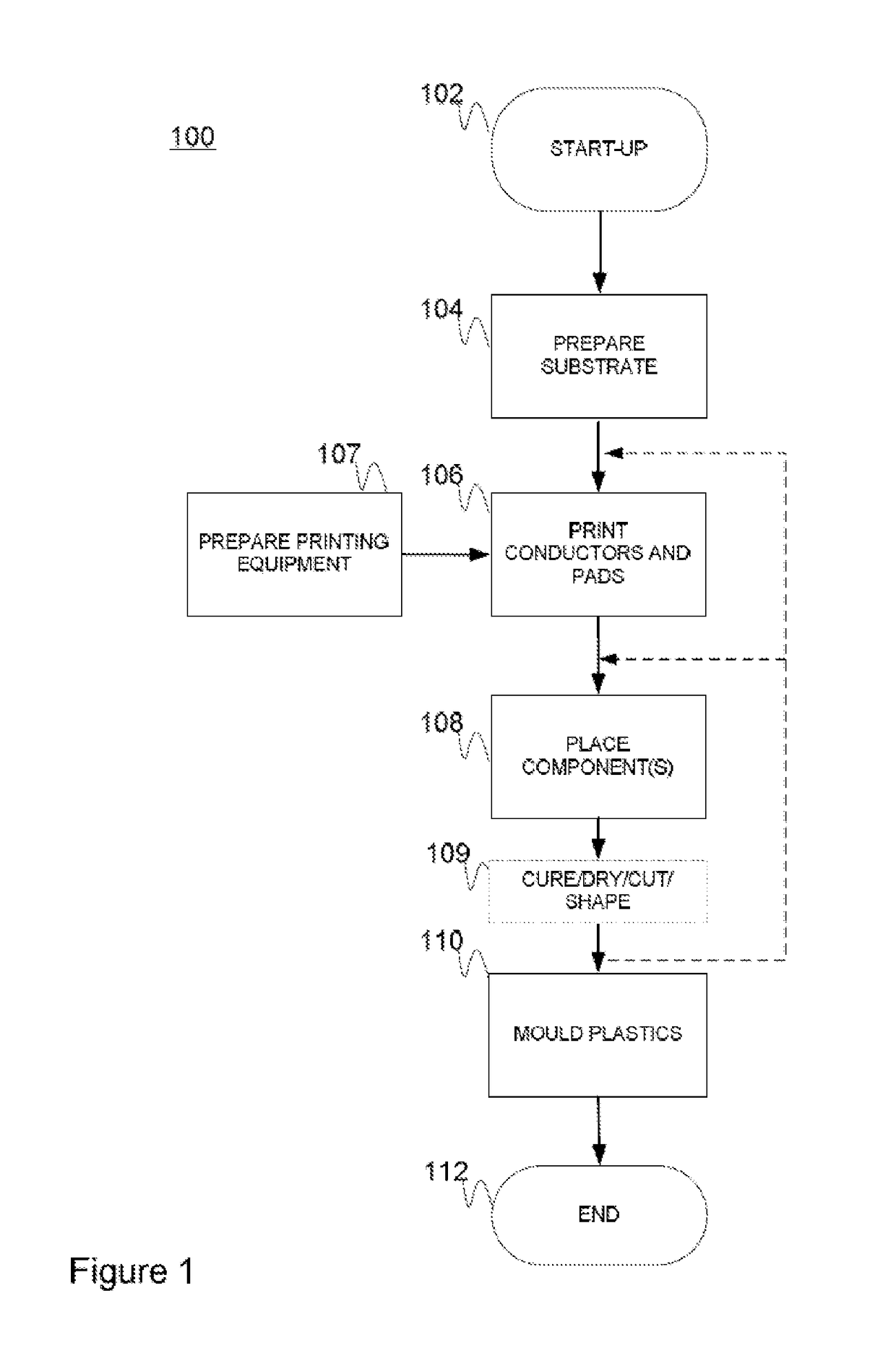
[0042]With reference to FIG. 1, a flow diagram of one feasible embodiment for manufacturing an electronic product, or device, in accordance with the present invention is shown.

[0043]At 102, referring to a start-up phase, the necessary preparatory actions such as material, element and tools general selection, acquisition and preprocessing take place. Circuit layout may be defined in the light of product specification and other constraints. Process parameters may be tested, tweaked and optimized.

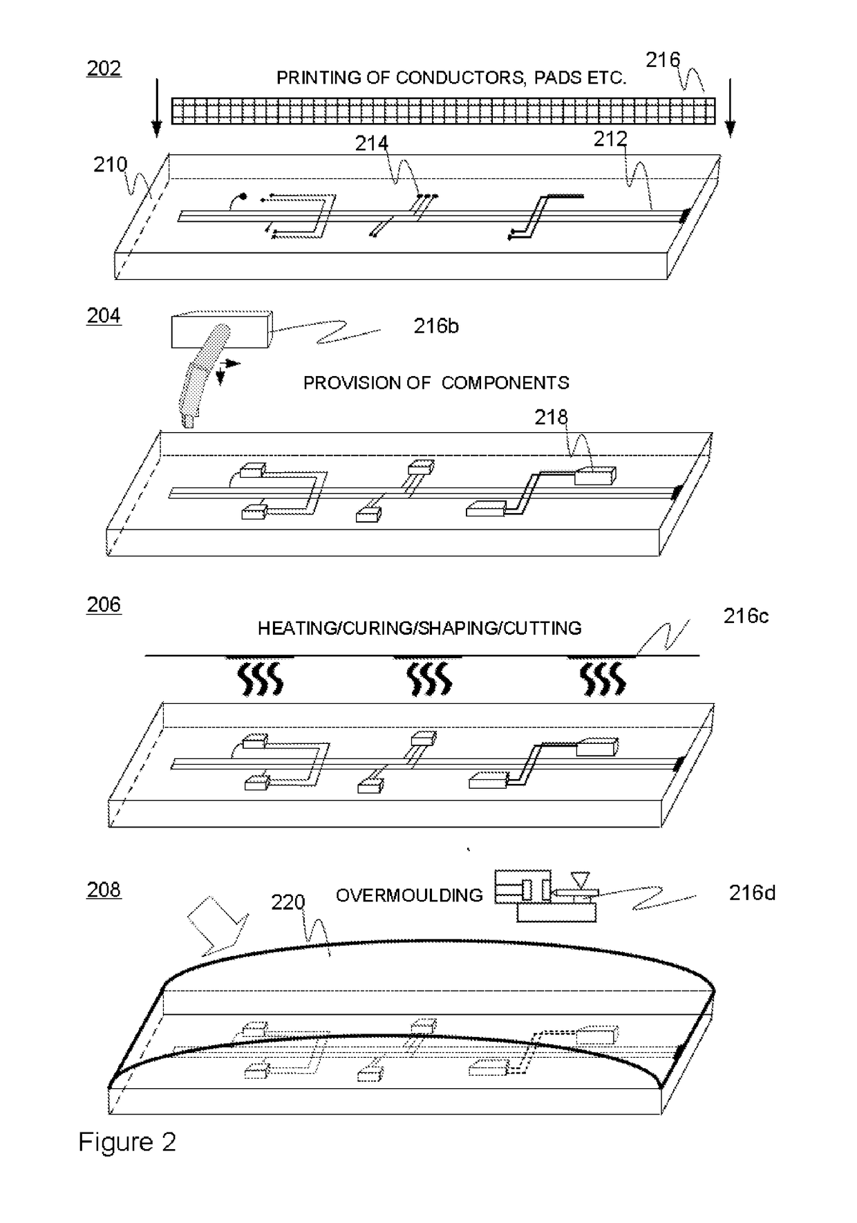
[0044]Conductive ink(s) is / are acquired. Examples of commonly available conductive inks include e.g. DuPont 5000™ and Asahi SW1600C™.

[0045]Advantageously, the selected inks are passive in contrast to e g many conductive adhesives, and bear rheological properties, e.g. viscosity or surface tension, which enable sufficient flow during ejection or squeezing, i.e. ink dispensing / printing, but prevent the ink from spreading too easily into adjacent materials and structures afterwards. Yet, drying c...


PUM

PropertyMeasurementUnit
thicknessaaaaaaaaaa
pressureaaaaaaaaaa
temperatureaaaaaaaaaa

Abstract

A method for manufacturing an electronic product, comprising providing a flexible, optionally optically substantially transparent or translucent, substrate film, printing a number of conductive traces of conductive ink on the substrate film, said traces defining a number of conductors and conductive contact areas for the contacts of at least one electronic surface-mountable component, disposing the at least one electronic surface-mountable component, such as an integrated circuit, on the substrate film so that the contacts meet the predefined contact areas when they are still wet to establish the electrical connection therebetween, and further securing, optionally overmoulding, the component. Related arrangement and electronic product are presented.

Description

FIELD OF THE INVENTION[0001]Generally the present invention concerns manufacturing processes in the context of electronic products. Particularly, however not exclusively, the invention pertains to manufacturing processes involving printed electronics and the usage of conductive inks.BACKGROUND[0002]Miniaturization is a prevalent trend in the manufacturing of electronic products. Additionally, manufacturing costs should be kept minimum, which implies relatively straightforward, high yield processes with reduced number of process stages and material waste among other factors.[0003]Although more traditional electronic elements such as PCBs (printed circuit board), conductors, components like SMDs (surface-mount device), etc. have reduced in size, many of them are still relatively bulky compared to printed electronics. Printed electronics have generally shown the way to thin, light, flexible and rapidly manufactured structures but a vast amount of components cannot still be manufactured...

Claims


Application Information

Patent Timeline
Patent Type & Authority Applications(United States)
IPC IPC(8): H05K3/12H05K1/18H05K3/28H05K1/02H05K1/09H05K3/00H05K3/30
CPCH05K2203/1316H05K1/189H05K1/181H05K3/305H05K3/284H05K3/1216H05K1/0284H05K2203/1105H05K2201/0108H05K3/12H05K3/0014H05K1/092Y10T29/53174
Inventor NISKALA, PAAVORAAPPANA, PASIHEIKKINEN, MIKKOSIPPARI, MIKKOTORVINEN, JARKKO
Owner TACTOTEK
Why Eureka
Try Eureka