

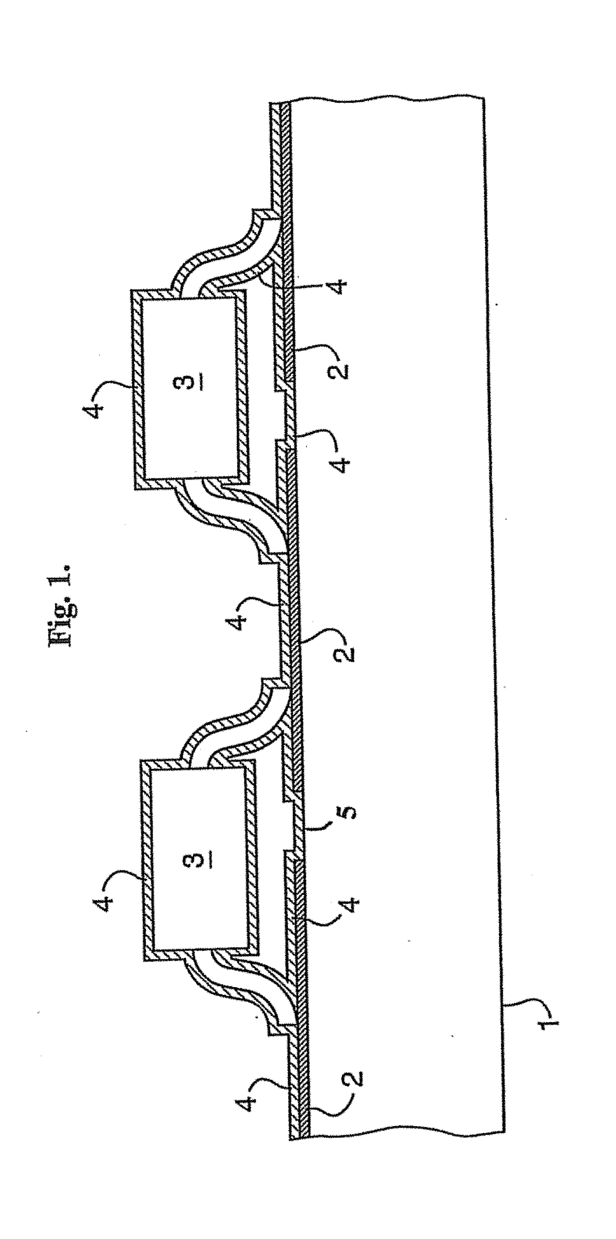
Coated electrical assembly
a technology of electrical components and coatings, applied in the direction of dielectric characteristics, non-metallic protective coating applications, association of printed circuit non-printed electrical components, etc., can solve the problems of time-consuming and expensive deposition process, high starting material cost, etc., and achieve excellent moisture-barrier properties, high level of chemical, electrical and physical protection, and high level of waterproofing
- Summary
- Abstract
- Description
- Claims
- Application Information
AI Technical Summary
Benefits of technology
Problems solved by technology
Method used
Image

Examples
example 1
Deposition of a Single SiOxCyHz Layer
[0103]An electrical assembly was placed into a plasma-enhanced chemical vapour deposition (PECVD) deposition chamber, and the pressure was then brought to −3 mbar. He was injected at a flow rate resulting in a chamber pressure of 0.480 mbar, then it was increased (by means of a throttle valve) to 0.50 mbar. Plasma was ignited at RF power of 45 W for 3-5 seconds. Next, HMDSO was injected into the chamber at a flow rate of 6 sccm and RF power density was at 0.225, 0.382, 0.573 or 0.637 Wcm−2 for 20 minutes. Pressure was kept (through a throttle valve) at 0.5 mbar during the deposition process.
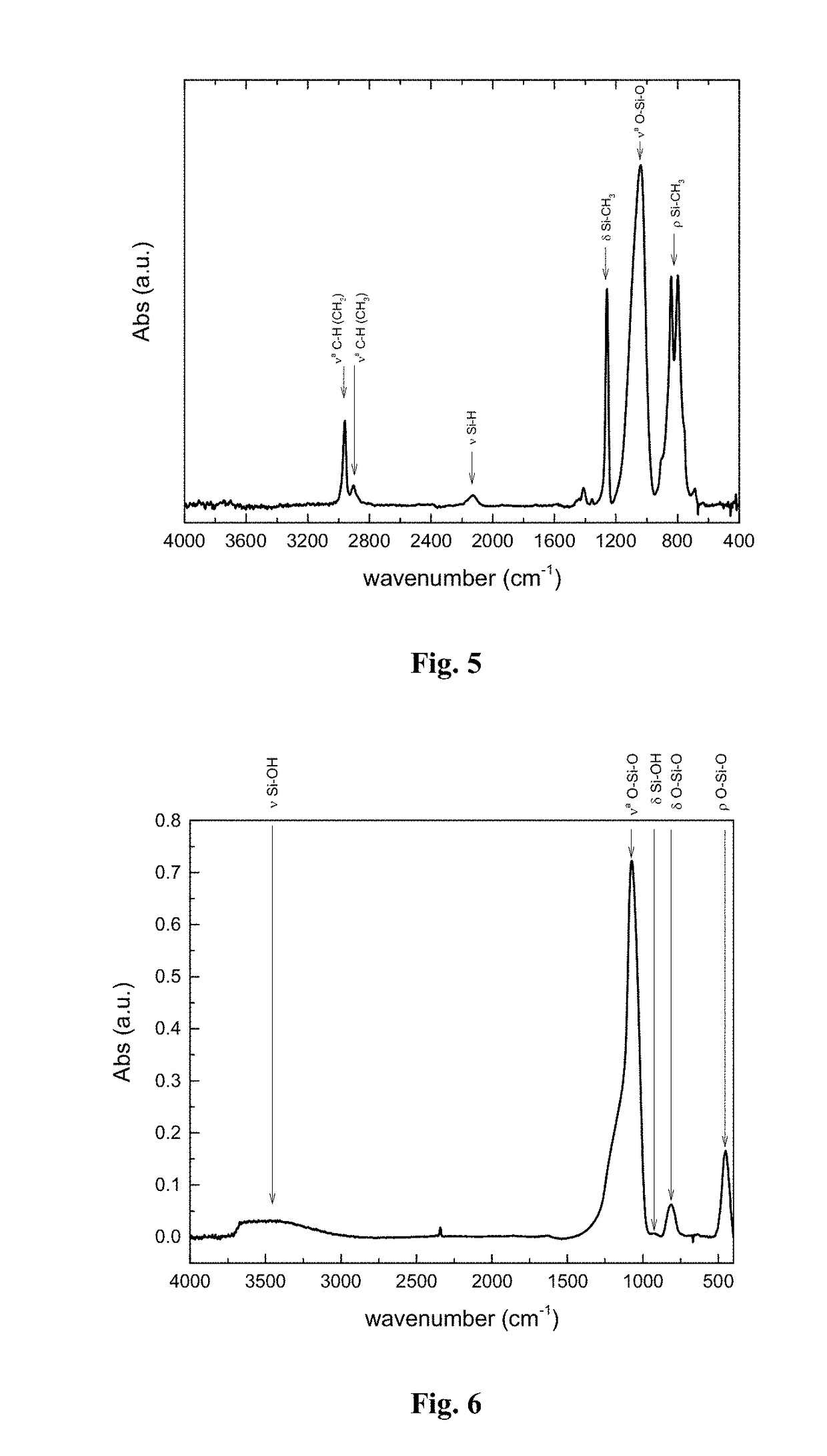
[0104]Polymeric organosilicon SiOxCyHz layers were obtained on the electrical assembly. The FT-IR transmission spectra for the layer obtained using an RF power density of 0.637 Wcm−2 is shown in FIG. 5.
[0105]The SiOxCyHz layers showed hydrophobic character with a WCA (water contact angle) of ˜100°.
[0106]The coated electrical assemblies (combs and pads) were te...
example 2
Deposition of Single SiOxHz Layer
[0107]An electrical assembly was placed into a PECVD deposition chamber, and the pressure was then brought to −3 mbar. Against this base pressure, O2 was inject up to 0.250 mbar of chamber pressure. After that, He was injected in order to reach a chamber pressure of 0.280 mbar. Finally, HMDSO was injected at a flow rate of 2.5 sccm and pressure was increased (by means of throttle valve) to 0.300 mbar. Plasma was then ignited with a power density of 0.892 Wcm−2 and the process was continued until the desired thickness of approximate 750 nm was achieved. A SiOxHz layer was obtained with FT-IR transmission spectrum as shown in FIG. 6. The SiOxHz layer showed hydrophilic character with a WCA ˜50°.
example 3
Deposition of SiOxCyHz / SiOxHz Multilayer
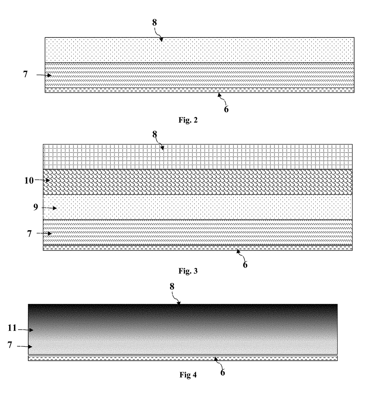
[0108]The experimental conditions leading to the PECVD deposition of the SiOxCyHz / SiOxHz multilayers on electrical assemblies were basically the same as described in Examples 1 and 2. Briefly, SiOxCyHz was deposited with the same procedure explained in Example 1 (RF power density used for this experiment was 0.637 Wcm−2), then chamber was brought to vacuum (−3 mbar) and the deposition of SiOxHz, on top of the SiOxCyHz layer, was performed according to the procedure explained in Example 2. Then, a second SiOxCyHz layer was deposited on top of the SiOxHz layer. The thickness of the second SiOxCyHz layer was half that of the first SiOxCyHz layer. This was achieved by halving the deposition time. These steps resulted in multilayer coating with the structure: SiOxCyHz / SiOxHz / SiOxCyHz.
[0109]The process was then repeated on some electrical assemblies in order to add a second pair of SiOxCyHz / SiOxHz layer, thereby giving the structure: SiOxCyHz / SiOxH...
PUM
| Property | Measurement | Unit |
|---|---|---|
| pressure | aaaaa | aaaaa |
| pressure | aaaaa | aaaaa |
| pressure | aaaaa | aaaaa |
Abstract
Description
Claims
Application Information