Iii-nitride tunnel junction light emitting diode with wall plug efficiency of over seventy percent

a technology of iiinitride and tunnel junction, which is applied in the direction of solid-state devices, lasers, semiconductor lasers, etc., can solve the problems of inability to use, and traditional p-contacts will add significant voltage to devices, so as to reduce loss, improve efficiency, and reduce droop

Active Publication Date: 2019-05-30
RGT UNIV OF CALIFORNIA
View PDF7 Cites 1 Cited by
  • Summary
  • Abstract
  • Description
  • Claims
  • Application Information

AI Technical Summary

Benefits of technology

[0014]To overcome the limitations described above, and to overcome other limitations that will become apparent upon reading and understanding this specification, the present invention described herein discloses a tunnel junction in a III-Nitride LED to increase efficienc

Problems solved by technology

However, the p-GaN is difficult to contact electrically and has low hole concentration and mobility, This means that p-

Method used


Image

  • Iii-nitride tunnel junction light emitting diode with wall plug efficiency of over seventy percent
  • Iii-nitride tunnel junction light emitting diode with wall plug efficiency of over seventy percent
  • Iii-nitride tunnel junction light emitting diode with wall plug efficiency of over seventy percent

Examples


example 1

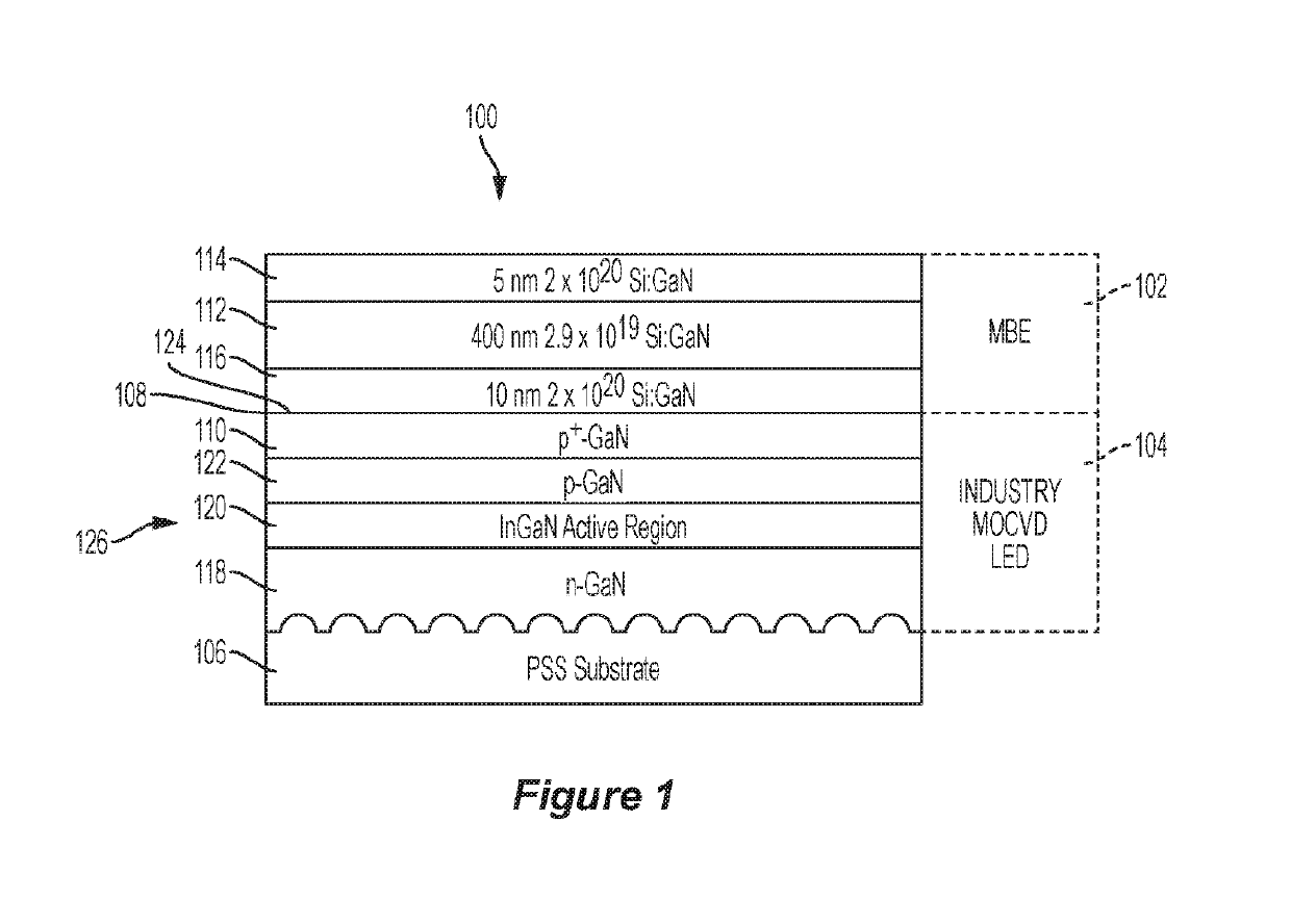
Transparent LED or PSS Lateral TJ LED Structure and Fabrication

[0061]A lateral LED is term used for LEDs that use ITO or ZnO for current spreading on the top layer.

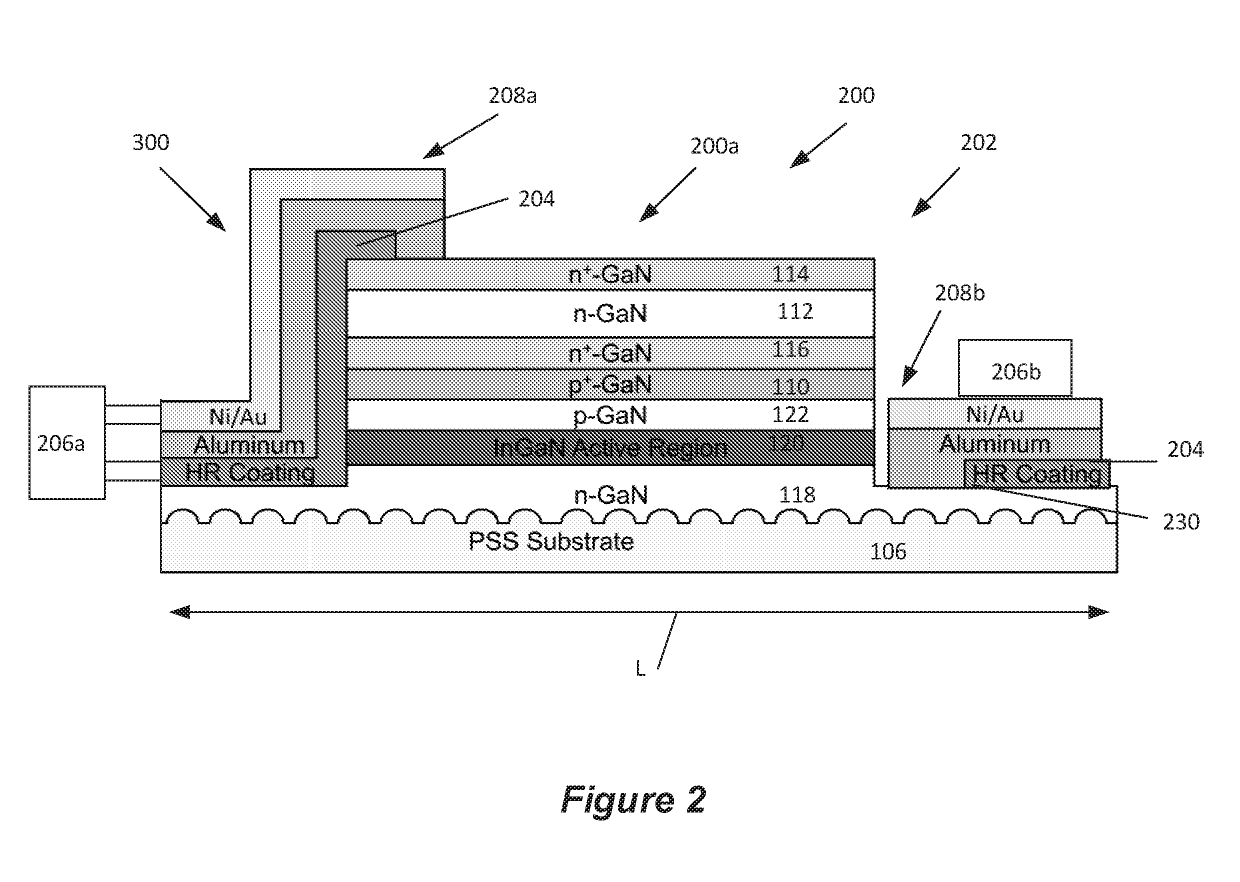
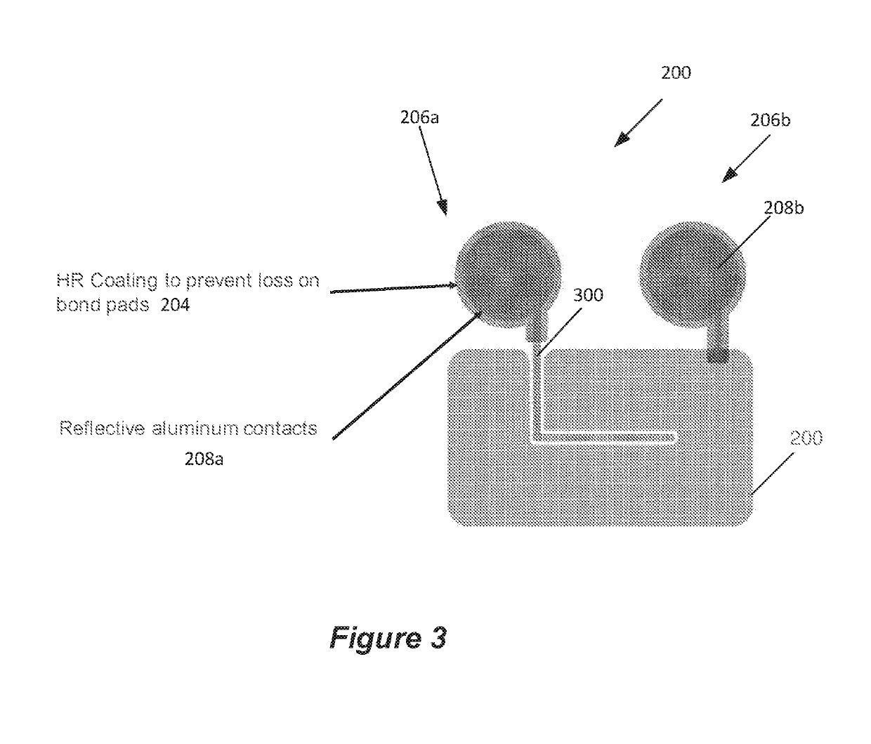
[0062]FIG. 2 illustrates the lateral tunnel junction LED 200 on a PSS substrate 106 and having a high reflective (HR) coating 204 under the wire bond pads 206a, 206b.

[0063]For the transparent LEDs 200 according to an embodiment of the present invention, a mesa 202 etch was first done using reactive ion etching (RIE) with SiCl4. A dielectric coating 204 was then deposited to reduce optical loss of the wire bond pads 206a, 206b. In one embodiments, the dielectric coating 204 comprises seven-layer dielectric stack consisting of Al2O3 / Ta2O5 / SiO2 was designed using TFCalc which increased the reflectivity of the wire bond pads 206a, 206b to over 98% at a wavelength of 450 nm. The topside wire bond pad 206a was also moved off the mesa 202 to prevent it from reflecting light (emitted under it) back into the chip 200a. A 600 / 200 / ...

example 2

Transparent Substrate Embodiment

[0069]FIG. 6 illustrates an embodiment wherein a transparent substrate is used to hold the LED. In an alternative embodiment, multiple LEDs could be used on the same substrate,

example 3

Back Reflector Embodiment

[0070]FIG. 7 illustrates a device embodiment 700 wherein a back reflector 702 (e.g., metal such as silver or aluminum) is used on the sapphire 106 to prevent loss on the header 406, and high reflective dielectric coating 704 is between the back reflector 702 (e.g., aluminum) and the substrate 106. Wire bonds 710 are also shown.

[0071]FIG. 8(a) shows the measured LIV characteristic (plotting light output power and voltage as a function of current) for the lateral TJ LED embodiment with back reflector illustrated in FIG. 7, wherein current is injected into an area of 0.1 mm2 (so that 1 mA drive current corresponds to 1 A / cm2 current density), FIG. 8(b) plots the measured EQE and WPE for this lateral tunnel junction LED embodiment (peak EQE is 78% and peak WPE is 72%).


PUM


Abstract

A III-Nitride LED which utilizes n-type III-Nitride layers for current spreading on both sides of the device. A multilayer dielectric coating is used underneath the wire bond pads, both LED contacts are deposited in one step, and the p-side wire bond pad is moved off of the mesa. The LED has a wall plug efficiency or External Quantum Efficiency (EQE) over 70%, a fractional EQE droop of less than 7% at 20 A/cm2 drive current and less than 15% at 35 A/cm2 drive current. The LEDs can be patterned into an LED array and each LED can have an edge dimension of between 5 and 50 μm. The LED emission wavelength can be below 400 nm and aluminum can be added to the n-type III-Nitride layers such that the bandgap of the n-type III-nitride layers is larger than the LED emission photon energy.

Description

CROSS REFERENCE TO RELATED APPLICATIONS[0001]This application claims the benefit under 35 U.S.C. Section 119(e) of co-pending and commonly-assigned U.S. Provisional Patent Application No. 62 / 376,218, filed on Aug. 17, 2016, by Benjamin P. Yonkee, Erin C. Young, James S. Speck, Steven P. DenBaars, and Shuji Nakamura, entitled “HI-NITRIDE TUNNEL JUNCTION LIGHT EMITTING DIODE WITH WALL PLUG EFFICIENCY OF OVER SEVENTY PERCENT,” Attorney's Docket No. 30794.627-US-P1 (UC Ref. 2017-131-1), which application is incorporated by reference herein.[0002]This application is related to the following co-pending and commonly-assigned U.S. patent applications:[0003]International PCT Application No. PCT / US17 / 16720 filed Feb. 6, 2017, entitled III-NITRIDE LIGHT EMITTING DIODES WITH TUNNEL JUNCTIONS WAFER BONDED TO A CONDUCTIVE OXIDE AND HAVING OPTICALLY PUMPED LAYERS, by Asad J. Mughal, Stacy J. Kowsz, Robert M. Farrell, Benjamin Yonkee, Erin C. Young, Christopher D. Pynn, Tal Margalith, James S. Spec...

Claims


Application Information

Patent Timeline
IPC IPC(8): H01L33/32H01L33/04H01L33/42H01L33/00H01S5/343
CPCH01L33/32H01L33/04H01L33/42H01L33/0075H01S5/343H01L33/14H01L33/20H01L33/385H01L2224/48091H01L2924/00014
Inventor YONKEE, BENJAMIN P.YOUNG, ERIN C.SPECK, JAMES S.DENBAARS, STEVEN P.NAKAMURA, SHUJI
Owner RGT UNIV OF CALIFORNIA
Why Eureka
Try Eureka