Bump structures for high density flip chip interconnection

a flip chip and structure technology, applied in the field of interconnections, can solve the problems of reducing the pitch size of the minimum, shortening the pixels, and affecting the smoothness of the flip chip, so as to reduce the overhang of the dielectric material layer

Active Publication Date: 2019-08-08
SENSORS UNLTD
View PDF0 Cites 11 Cited by
  • Summary
  • Abstract
  • Description
  • Claims
  • Application Information

AI Technical Summary

Benefits of technology

[0004]A method of forming bump structures for interconnecting components includes applying an insulating layer over a device substrate, coating the insulating layer with a dielectric material layer, forming a pattern with photolithography on the dielectric material layer, etching the dielectric material layer to transfer the pattern to the insulating layer, etching the insulating layer to form pockets in the insulating layer following the pattern, applying photolithography to and etching the dielectric material layer to reduce overhang of the dielectric material layer relative to the insulating layer, removing material from top and side walls of the pockets in the insulating layer, and depositing electrically conductive bump material in the pattern so a respective bump is formed in each pocket.

Problems solved by technology

However, due to the bowing of the dies, especially for large sized FPAs, the misalignment caused by the lateral shifting becomes more significant.
The lateral expansion of the bumps during the hybridization process could cause the shortage with the neighbor bumps, which result in the shorting pixels.
The minimization of pitch sizes is therefore limited.
The wicking process also becomes more challenging as die size increases and pitch sizes become finer.

Method used


Image

  • Bump structures for high density flip chip interconnection
  • Bump structures for high density flip chip interconnection
  • Bump structures for high density flip chip interconnection

Examples


Embodiment Construction

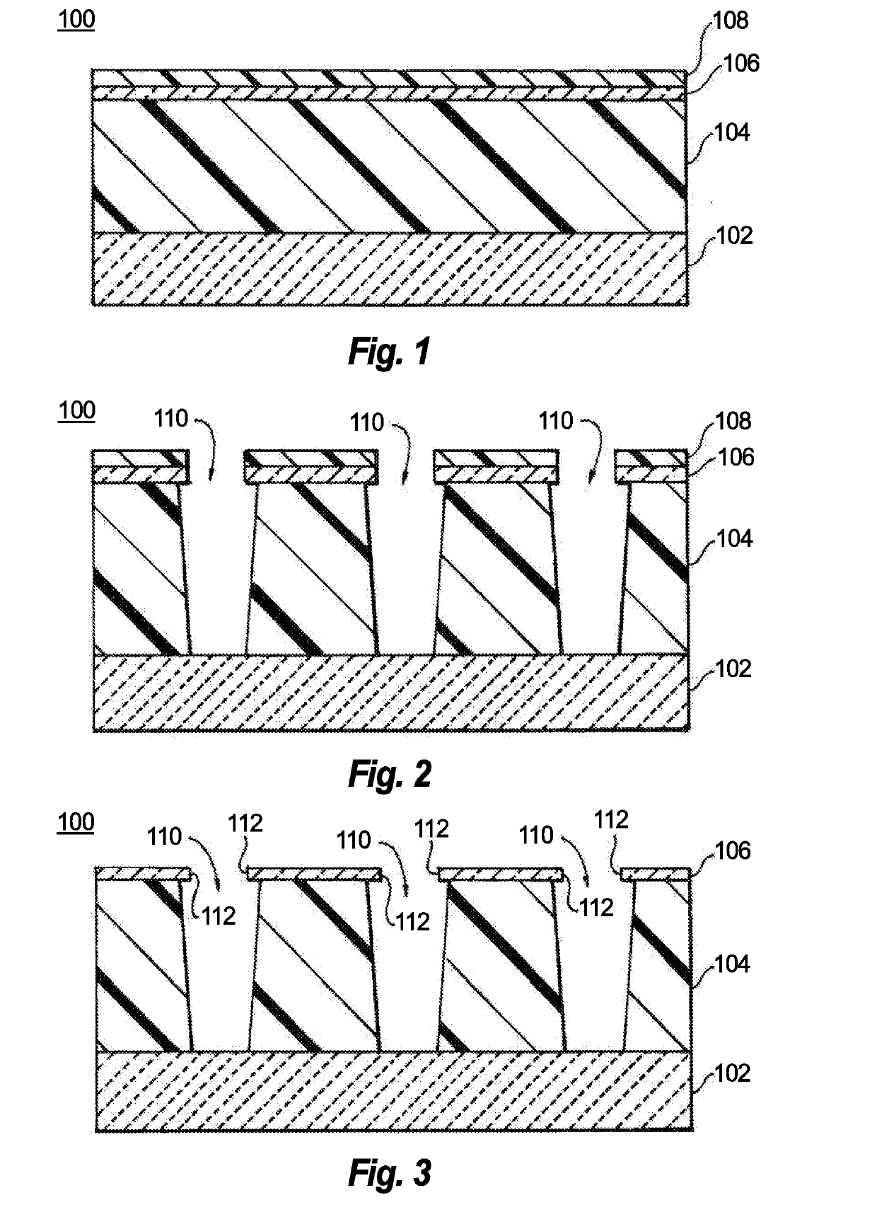
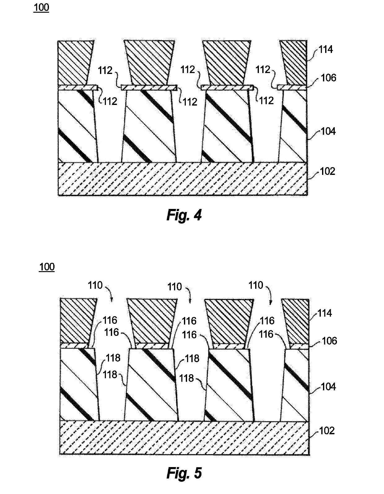
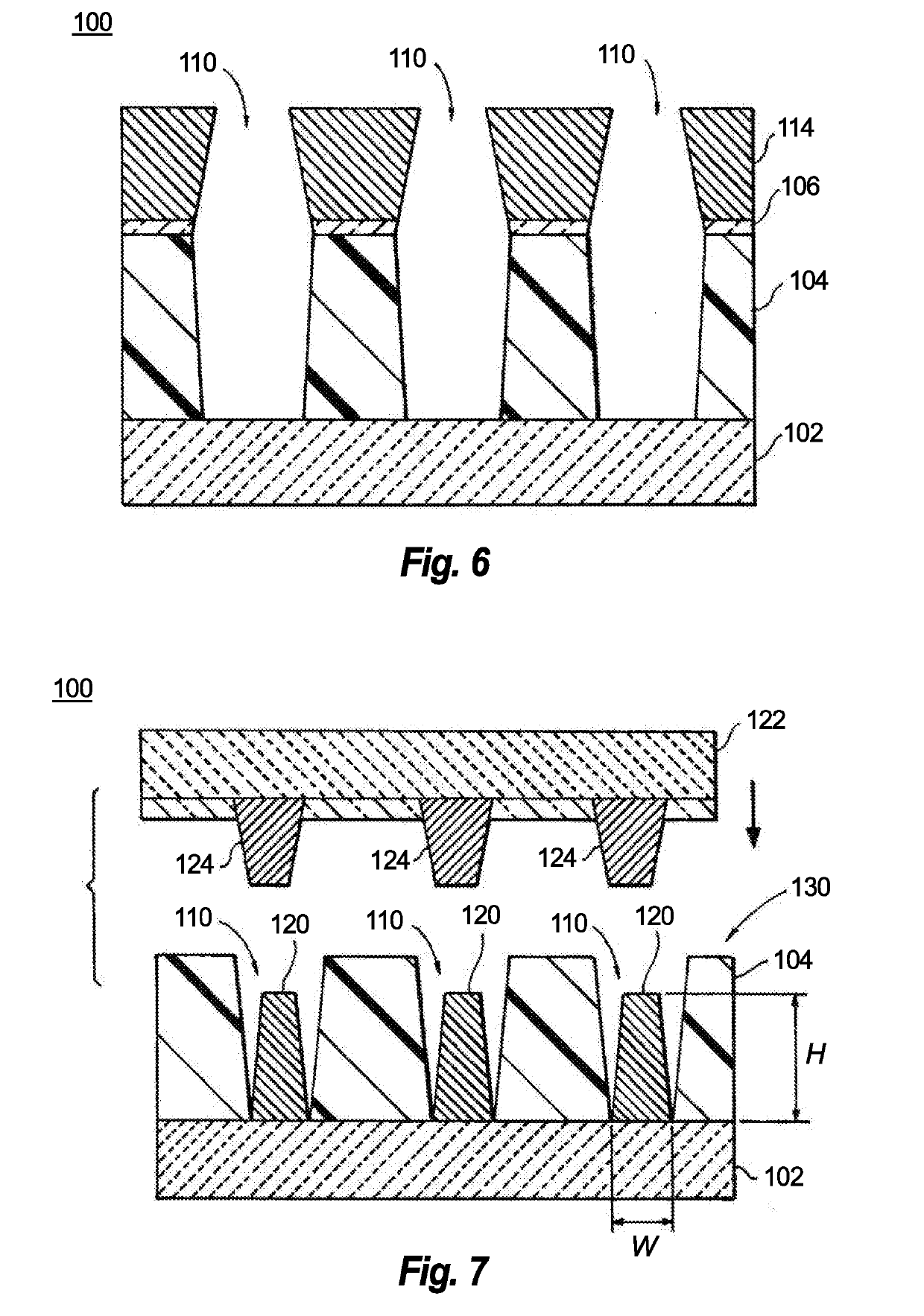
[0020]Reference will now be made to the drawings wherein like reference numerals identify similar structural features or aspects of the subject disclosure. For purposes of explanation and illustration, and not limitation, a partial view of an exemplary embodiment of a system in accordance with the disclosure is shown in FIG. 1 and is designated generally by reference character 100. Other embodiments of systems in accordance with the disclosure, or aspects thereof, are provided in FIGS. 2-8, as will be described. The systems and methods described herein can be used for interconnections in focal plane arrays (FPAs) and the like.

[0021]A method of forming bump structures for interconnecting components includes applying an insulating layer 104 over a device substrate 102 and coating the insulating layer 104 with a dielectric material layer 106. The insulating layer 104 can include at least one of polymethyl methacrylate (PMMA) and / or Polyimide, and can be applied to be at least 5 μm thic...


PUM

PropertyMeasurementUnit
width aspect ratioaaaaaaaaaa
thickaaaaaaaaaa
pressureaaaaaaaaaa

Abstract

A method of forming bump structures for interconnecting components includes applying an insulating layer over a device substrate, coating the insulating layer with a dielectric material layer, forming a pattern with photolithography on the dielectric material layer, etching the dielectric material layer to transfer the pattern to the insulating layer, etching the insulating layer to form pockets in the insulating layer following the pattern, applying photolithography to and etching the dielectric material layer to reduce overhang of the dielectric material layer relative to the insulating layer, removing material from top and side walls of the pockets in the insulating layer, and depositing electrically conductive bump material in the pattern so a respective bump is formed in each pocket.

Description

BACKGROUND OF THE INVENTION1. Field of the Invention[0001]The present disclosure relates to interconnections, and more particularly to bump structures for electrically interconnecting components such as in interconnecting focal plane array components.2. Description of Related Art[0002]For small pixel pitch Focal Plane Array (FPA) application, flip chip hybridization provides advantages over the wire bonding process, such as high I / O density and short interconnect distance between the photodiode array (PDA) and the readout integrated circuit (ROIC), which lead to high device performance and miniature devices. Indium has become the ideal mating material because of its high ductility at low temperature. However, due to the bowing of the dies, especially for large sized FPAs, the misalignment caused by the lateral shifting becomes more significant. The lateral expansion of the bumps during the hybridization process could cause the shortage with the neighbor bumps, which result in the sh...

Claims


Application Information

Patent Timeline
Patent Type & Authority Applications(United States)
IPC IPC(8): H01L23/00H01L21/48H01L23/13H01L27/146
CPCH01L24/14H01L21/4857H01L23/13H01L21/4853H01L24/11H01L24/81H01L27/14643H01L23/49816H01L27/1469H01L27/14636H01L2224/83201H01L2224/83203H01L2224/81895H01L2224/1148H01L2224/11472H01L2224/81193H01L2224/16145H01L2224/32145H01L2924/12043H01L2224/13109H01L24/13H01L2224/13005H01L2224/81141H01L2224/1145H01L2224/13017H01L2224/83903H01L2224/13023H01L2224/13021H01L2224/73103H01L24/16H01L24/29H01L24/32H01L24/27H01L2224/2919H01L2224/29011H01L2224/29017H01L2224/81201H01L2224/81203H01L2224/9211H01L2224/9212H01L24/73H01L24/92H01L24/83H01L2224/83141H01L2224/83191H01L2224/27612H01L2224/1147H01L2224/119H01L2224/279H01L2924/00014H01L2924/00012H01L2224/81H01L2224/83H01L2224/27H01L2224/11
Inventor ZHANG, WEIHUANG, WEILUND, JOSHUAPAIK, NAMWOONG
Owner SENSORS UNLTD
Why Eureka
Try Eureka