Imaging devices, camera modules, and fabrication methods thereof

a camera module and imaging device technology, applied in the direction of semiconductor devices, semiconductor/solid-state device details, radiation controlled devices, etc., can solve the problems of not being able to use any traditional package cleaning method to remove remaining dust or other foreign objects, and the overall production yield of the cmos camera module may be seriously affected

Inactive Publication Date: 2019-08-08
SHANGHAI JUEXIN PHOTOELECTRIC TECH CO LTD
View PDF0 Cites 0 Cited by
  • Summary
  • Abstract
  • Description
  • Claims
  • Application Information

AI Technical Summary

Problems solved by technology

Since the color micro-filter array and the micro-lens array are both made of a polymer, it may not be easy to use any traditional package cleaning method to remove the remaining and residual dust or other foreign objects.
Therefore, once dust or o...

Method used


Image

  • Imaging devices, camera modules, and fabrication methods thereof
  • Imaging devices, camera modules, and fabrication methods thereof
  • Imaging devices, camera modules, and fabrication methods thereof

Examples


Embodiment Construction

[0017]Reference will now be made in detail to exemplary embodiments of the invention, which are illustrated in the accompanying drawings. Wherever possible, the same reference numbers will be used throughout the drawings to refer to the same or like parts.

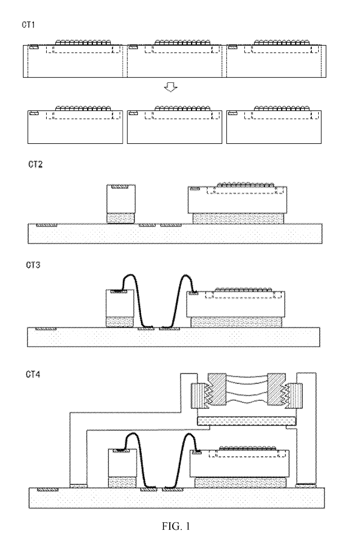
[0018]FIG. 1 illustrates schematic views of semiconductor structures at certain stages of an existing assembly process for a CMOS camera module. Referring to FIG. 1, the assembly process includes the following steps:

[0019]CT1: cutting a wafer of CMOS image sensor chips into a plurality of separate CMOS image sensor chips;

[0020]CT2: attaching an individual CMOS image sensor chip and auxiliary devices to a base substrate, the base substrate including a multi-layer printed circuit board (PCB) or a flexible printed circuitry (FPC);

[0021]CT3: forming interconnections between the CMOS image sensor chip, the auxiliary devices, and the base substrate through wire bonding;

[0022]CT4: placing and sealing a prefabricated modular assembly of le...


PUM


Abstract

An imaging device includes an image sensor chip. The image sensor chip includes a photosensitive surface and, opposite to the photosensitive surface, a bottom surface. The photosensitive surface includes a sensitive region, a peripheral transition region surrounding the photosensitive region, and an input/output wiring region surrounding the peripheral transition region. At least one input/output wiring pad is disposed in the input/output wiring region. The imaging device also includes a selective filter cover, disposed above the photosensitive region; and a retaining wall, disposed in the peripheral transition region and bonded to the selective filter cover. The retaining wall and the selective filter cover together form a closed cavity above the photosensitive region. The imaging device further includes a plurality of outgoing wires. A terminal of each outgoing wire is connected to an input/output wiring pad, and another terminal of the outgoing wire extends out from the image sensor chip.

Description

CROSS-REFERENCES TO RELATED APPLICATIONS[0001]This application claims the priority of Chinese Patent Application No. CN201810113956.0, filed on Feb. 5, 2018, the entire content of which is incorporated herein by reference.FIELD OF THE DISCLOSURE[0002]The present disclosure generally relates to the field of semiconductor fabrication technology and, more particularly, relates to imaging devices, camera modules, and fabrication methods thereof.BACKGROUND[0003]Compared with the charge-coupled device (CCD) camera module, the complementary metal-oxide-semiconductor (CMOS) camera module (CCM) demonstrates the advantages of small size and low power consumption. Today, high-performance, miniaturized CMOS camera modules and the corresponding image processing functions have become essential ingredients for smartphones. In addition, with intelligent identification functions, three-dimensional (3D) imaging cameras of mobile phones have also entered the commercial application stage. The resolutio...

Claims


Application Information

Patent Timeline
IPC IPC(8): H01L27/146H01L23/00
CPCH01L27/14634H01L27/14618H01L27/14621H01L27/14627H01L27/14636H01L27/14645H01L24/48H01L27/14687H01L27/1469H01L2224/48227H04N23/54H01L2924/00014H01L27/14625H01L27/14632H01L2224/48138H01L2224/24137H01L2224/24101H01L2224/96H01L24/24H01L2224/32225H01L2224/73265H01L2224/45099H01L2224/82H01L2924/00
Inventor WANG, XIAOCHUAN
Owner SHANGHAI JUEXIN PHOTOELECTRIC TECH CO LTD
Why Eureka
Try Eureka