Photosensitive device with electric shutter

a technology of photosensitive devices and shutters, applied in the direction of photometry using electric radiation detectors, optical radiation measurement, instruments, etc., can solve the problems of inability to achieve mechanical shutters, inability to prepare two separate elements in one pixel, and inability to achieve photodetector applications, etc., to facilitate the use of cds methods and high frame rate

Active Publication Date: 2019-09-26
EMBERION OY
View PDF0 Cites 10 Cited by
  • Summary
  • Abstract
  • Description
  • Claims
  • Application Information

AI Technical Summary

Benefits of technology

[0009]The disclosure is based on the fact that certain two-dimensional materials, such as graphene, demonstrate ambipolar conduction. Voltages applied through a gate electrode to a graphene field-effect transistor can therefore switch its carrier type from p-type to n-type and vice versa. It is also based on the realization that an insulated gate electrode can influence the interface voltage of the junction between the graphene layer and the photoactive layer, due to the limited number of energy states near the charge neutrality point in graphene. This allows the gate voltage to simultaneously change both the conduction type of the graphene layer and the interface voltage. The disclosure is further based on the surprising discovery that, if the graphene layer and the photoactive layer are prepared with suitable properties, the charge neutrality point of the graphene layer will lie at a gate voltage which allows an electrical shutter function to be performed by the gate electrode.
[0010]This electrical reset always resets a photosensitive transistor pixel to a known electrical state, so that even non-ideal effects with long time-constants are quickly neutralized. The reset time is short, which facilitates the use of the CDS method and a high frame rate in light detection applications.

Problems solved by technology

However, it is not an optimal solution to prepare two separate elements in one pixel.
However, there are many photodetector applications where mechanical shutters are not feasible.
Furthermore, mechanical shutters can often only perform an incomplete reset.

Method used


Image

  • Photosensitive device with electric shutter
  • Photosensitive device with electric shutter
  • Photosensitive device with electric shutter

Examples


first device embodiment

[0050]The photosensitive device may be a transistor which comprises at least one electrically conducting source electrode and at least one electrically conducting drain electrode in contact with the ambipolar two-dimensional material. When the device is a transistor, the control unit may be configured to apply a source-drain voltage between the at least one source electrode and the at least one drain electrode. Alternatively, the control unit may be configured to measure the electric potential of the ambipolar two-dimensional material through the source electrode and / or the drain electrode.

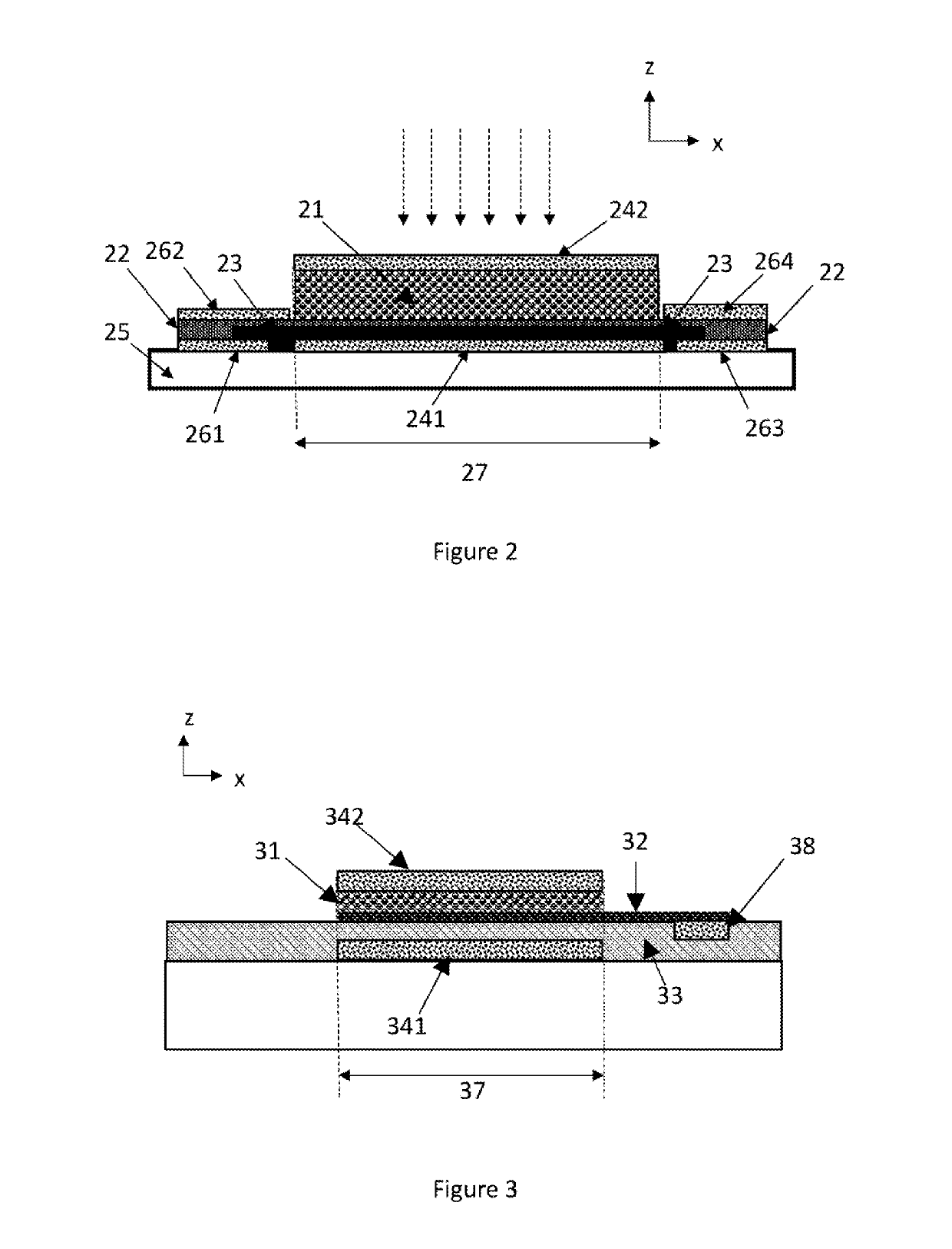
[0051]FIG. 2 illustrates an exemplary photosensitive transistor according to this first device embodiment. The transistor comprises a layer of photoactive semiconducting material 21, a graphene channel 22, a gate insulator 23, a bottom gate electrode 241 and a top gate electrode 242. The transistor further comprises two source electrodes 261 and 262, and two drain electrodes 263 and 264. The devic...

second device embodiment

[0063]The photosensitive device may be a voltage-mode device which comprises a single-ended measurement electrode in contact with the ambipolar two-dimensional material. The control unit may be configured to measure the electric potential of the ambipolar two-dimensional material through the measurement electrode. In this embodiment, source and drain electrodes are not used because no current needs to be driven through the ambipolar two-dimensional material.

[0064]FIG. 3 illustrates a voltage-mode device which comprises a photoactive semiconducting material 31, a graphene sensing electrode 32, a bottom gate electrode 341 and a top gate electrode 342. A layer of insulating material 33 separates the bottom gate electrode from the graphene sensing electrode 32. A single-ended measurement electrode 38 is used to measure the electric potential of the sensing electrode 32. The gate electrodes define a first region 37. The interface between the photoactive semiconducting material 31 and the...

first measurement embodiment

[0104]When a transistor structure is utilized in the photosensitive device, the control unit may be configured to measure the source-drain current between the at least one source electrode and the at least one drain electrode as the electrical response of the photosensitive device. The control unit may first set the source-drain current through the ambipolar two-dimensional material to an initial value, and the influence of injected charge carriers released by radiation in the photoactive semiconducting layer can then be detected as a deviation in the source-drain current from this initial value. A nearly simultaneous measurement of the dark current when the device is in the light-immune state provides a reference point for the measured photoinduced current, so that measurement noise is reduced in the calculated response. The response can then be used to calculate the intensity of the radiation incident on the photosensitive device after calibration experiments have been performed.

[...


PUM


Abstract

A photosensitive transistor or voltage-mode device which comprises a gate electrode, a layer of ambipolar two-dimensional material such as graphene and a layer of photoactive semiconducting material forms a junction with the ambipolar two-dimensional material. The photoactive semiconducting material and the ambipolar two-dimensional material are configured so that there is a non-screening gate voltage interval where an interface voltage at the junction between the photoactive semiconducting layer and the ambipolar two-dimensional material can be changed by applying to the gate electrode a gate voltage which falls within the non-screening gate voltage interval. The non-screening gate voltage interval comprises a flat-band gate voltage at which the interface voltage is zero. An electrical shutter can be operated at this gate voltage.

Description

FIELD OF THE DISCLOSURE[0001]This disclosure relates to photosensitive devices prepared on the surface of a substrate, and more particularly to devices which can be used for detecting the intensity of electromagnetic radiation. The present disclosure further concerns methods for measuring electromagnetic radiation with such devices, and methods for resetting such devices between successive measurements.BACKGROUND OF THE DISCLOSURE[0002]Field-effect transistors which utilize two-dimensional materials in the transistor channel, and voltage-mode devices which utilize two-dimensional materials as sensing electrodes can be used as versatile detectors of electromagnetic radiation at wavelengths ranging from infrared to ultraviolet. Such devices may be called photosensitive devices. A graphene field-effect transistor (GFET), for example, comprises a semiconducting graphene channel. Its conductivity can be measured, and strongly amplified, in a field-effect transistor geometry where the cur...

Claims


Application Information

Patent Timeline
Patent Type & Authority Applications(United States)
IPC IPC(8): H01L31/113H01L31/0352H01L31/028G01J1/44H04N25/60
CPCH01L31/028H01L31/1136G01J1/44H01L31/035281G01J1/42G01J1/044G01J1/0209H01L31/1121H01L31/0264H04N25/60
Inventor BESSONOV, ALEXANDERCOLLI, ALANALLEN, MARK
Owner EMBERION OY
Why Eureka
Try Eureka