
Method for optical interconnection between semiconductor chips using mid-infrared

a semiconductor chip and optical interconnection technology, applied in the direction of electromagnetic transmission, semiconductor lasers, transmission, etc., can solve the problems of high process cost, inefficient integration of circuits into a smaller size, difficult stacking a predetermined number of layers or more, etc., to reduce bandwidth and power consumption, low yield, and high cost

Active Publication Date: 2019-10-10
KOREA INST OF SCI & TECH
View PDF21 Cites 2 Cited by
  • Summary
  • Abstract
  • Description
  • Claims
  • Application Information

AI Technical Summary

Benefits of technology

The present patent text describes a new technology for optical interconnection between semiconductor chips that solves limitations of current technology, such as limited stacks and high cost. This technology uses a mid-infrared wavelength range of light that is transparent to semiconductor materials, allowing for interconnection without using metal wiring. The use of optical interconnection also avoids the need for substrate perforation and alignment processes, reducing process difficulty and cost, and extending the existing photonics technology platform to reduce design costs.

Problems solved by technology

Recently, with the development of semiconductor process and integration technology, it is possible to implement a multifunctional chip on a die in 1 cm×1 cm size, but integration of circuits into a smaller size is inefficient due to a very high process cost.
Accordingly, to overcome the limitation of the existing integration technology, studies have been made on 3-dimensional (3D) stack technology in many aspects to stack many semiconductor chips with a view of realizing more complex and delicate functions, but the technical limitation of interconnection between semiconductor chips makes it difficult to stack a predetermined number of layers or more.
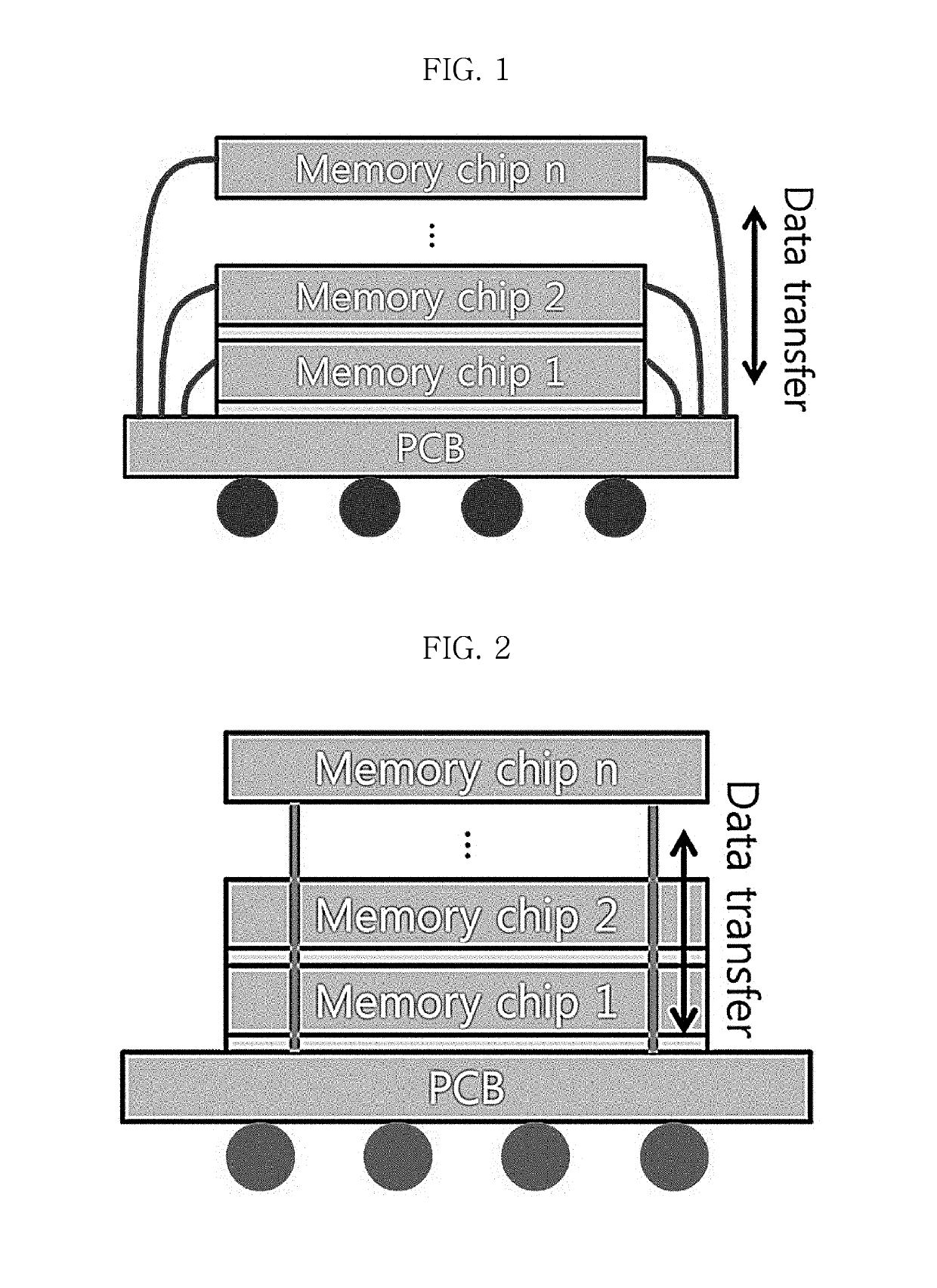
Wire bonding technology shown in FIG. 1 involves stacking each independent semiconductor chip bonded using a metal wire, and as the number of semiconductor chips stacked is larger, wiring is more complex, and there are technical problems caused by wiring, such as interference and heat generation.
However, the existing TSV technology is difficult to stack a predetermined number of layers or more due to the high cost and low yield problems, and because interconnection is impossible when each semiconductor chip is not correctly aligned, it is more sensitive to a manufacturing error than the wire bonding process.
Further, similar to the wire bonding process, as the number of stacks increases, the interconnection bandwidth increases, failing to cope with.
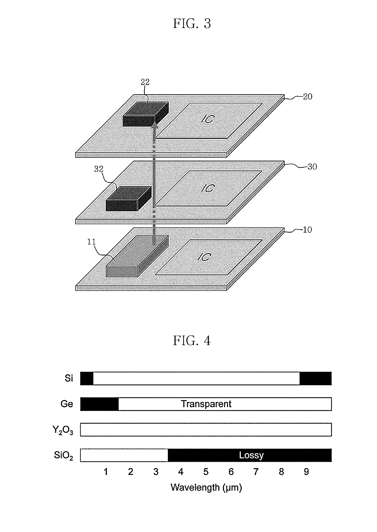
However, a wavelength range (for example, 1.3 μm, 1.55 μm) of light generally used for interconnection is blocked / absorbed by next-generation semiconductor materials having high mobility such as SiGe, Ge and lnGaAs, and a wavelength range of light generally used for interconnection fails to enable optical interconnection in semiconductor, requiring a separate structure for complex optical wiring.

Method used


Image

  • Method for optical interconnection between semiconductor chips using mid-infrared
  • Method for optical interconnection between semiconductor chips using mid-infrared
  • Method for optical interconnection between semiconductor chips using mid-infrared

Examples


Embodiment Construction

[0032]The following detailed description of the present disclosure is made with reference to the accompanying drawings, in which particular embodiments for practicing the present disclosure are shown for illustration purposes. These embodiments are described in sufficiently detail for those skilled in the art to practice the present disclosure. It should be understood that various embodiments of the present disclosure are different but do not need to be mutually exclusive. For example, particular shapes, structures and features described herein in connection with one embodiment can be embodied in other embodiment without departing from the spirit and scope of the present disclosure. It should be further understood that changes can be made to locations or arrangements of individual elements in each disclosed embodiment without departing from the spirit and scope of the present disclosure. Accordingly, the following detailed description is not intended to be taken in limiting senses, ...


PUM


Abstract

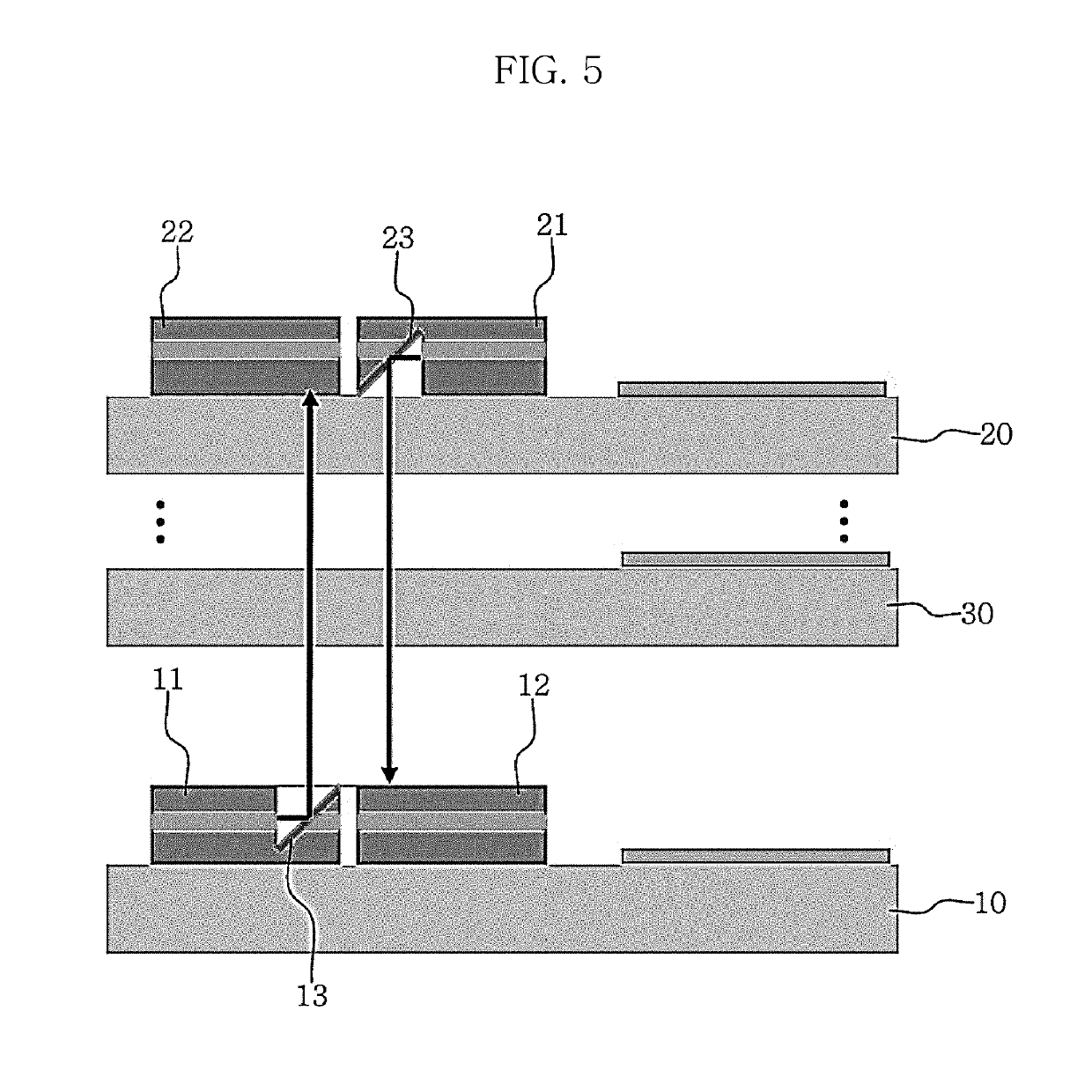
A method for optical interconnection between semiconductor chips according to an embodiment include converting an electrical signal to an optical signal, transmitting the optical signal to a second substrate disposed above or below a first substrate using an optical transmitter provided on the first substrate, receiving the optical signal using an optical detector provided on the second substrate, and converting the received optical signal to an electrical signal. Accordingly, using a mid-infrared wavelength range of light that is transparent to semiconductor materials such as silicon and next-generation high-mobility materials, it is possible to enable interconnection between stacked semiconductor chips without using metal wiring. Using optical interconnection, it is possible to significantly reduce the bandwidth and power consumption, and overcome the limitations of TSV technology, and it is possible to extend the photonics technology and platform established in the existing Si Photonics, thereby reducing the cost required for design.

Description

CROSS-REFERENCE TO RELATED APPLICATION[0001]This application claims priority to Korean Patent Application No. 10-2018-0039807, filed on Apr. 5, 2018, and all the benefits accruing therefrom under 35 U.S.C. § 119, the contents of which in its entirety are herein incorporated by reference.BACKGROUND1. Field[0002]The present disclosure relates to a method for optical interconnection between semiconductor chips using mid-infrared, and more particularly, to a technology of optical interconnection between semiconductor chips by transmission and reception of a mid-infrared wavelength range of light passing through silicon in a multilayer silicon substrate structure.2. Description of the Related Art[0003]A silicon (Si) substrate is widely used to fabricate a semiconductor device or an integrated circuit. Recently, with the development of semiconductor process and integration technology, it is possible to implement a multifunctional chip on a die in 1 cm×1 cm size, but integration of circuit...

Claims


Application Information

Patent Timeline
Patent Type & Authority Applications(United States)
IPC IPC(8): H04B10/80H04B10/66H04B10/50
CPCH04B10/801H04B10/66H04B10/503H01S5/0207H01S5/183H01S5/32391H04B10/803H01L2225/06534
Inventor HAN, JAEHOONKIM, SANGHYEONJU, HYUNSUSONG, JIN-DONG
Owner KOREA INST OF SCI & TECH
Learn More