

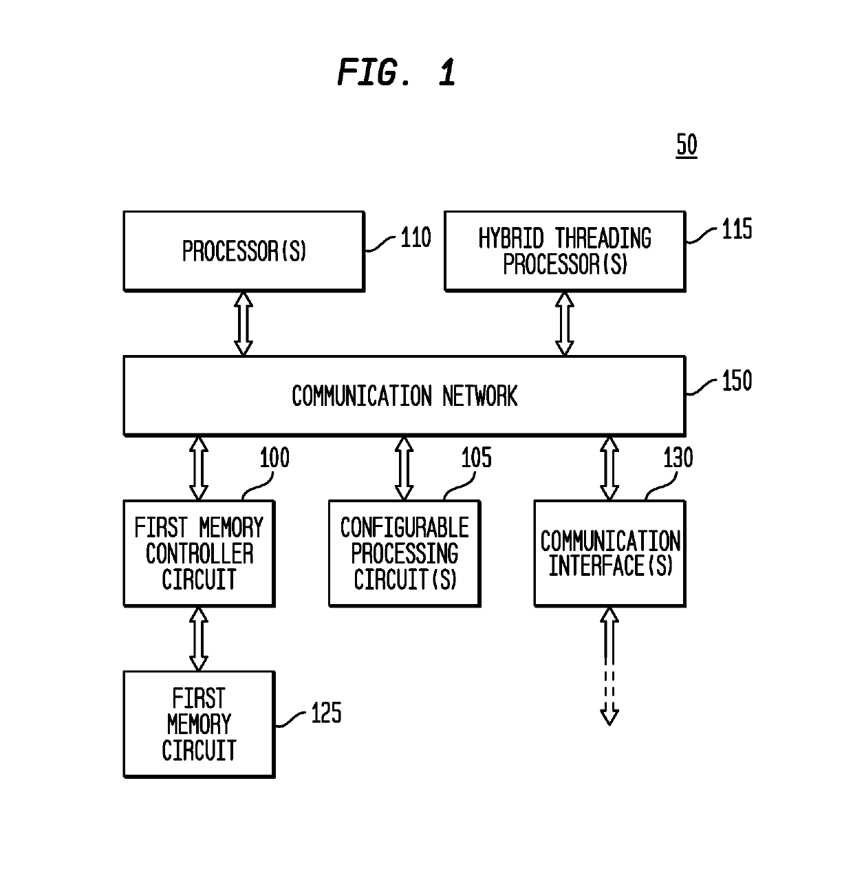
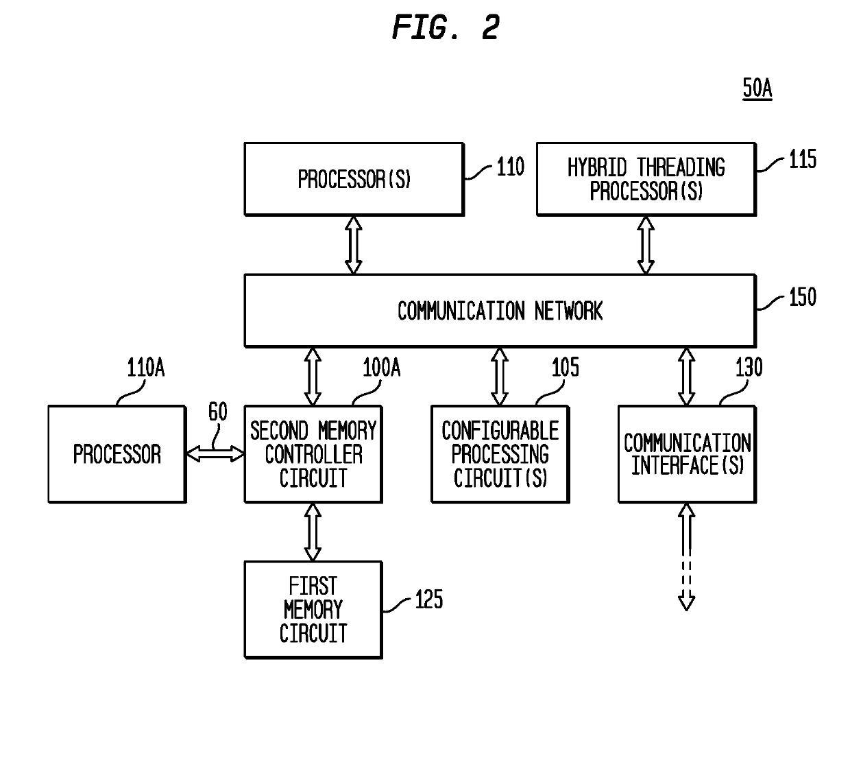
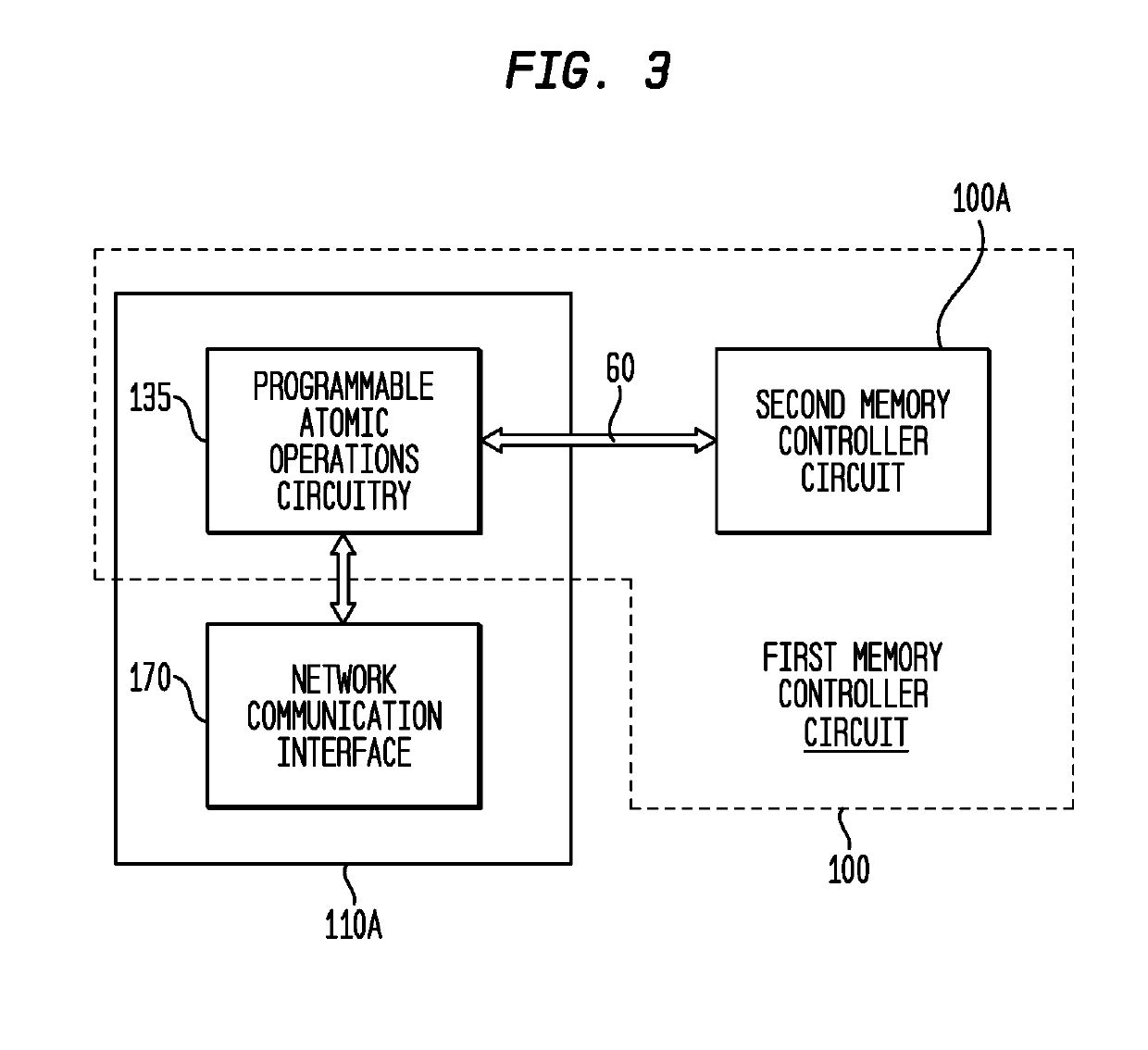
Memory Controller with Programmable Atomic Operations
a memory controller and atomic operation technology, applied in the field of memory controllers, can solve problems such as flat latency, and achieve the effects of high throughput, high performance and energy efficiency
- Summary
- Abstract
- Description
- Claims
- Application Information
AI Technical Summary
Benefits of technology
Problems solved by technology
Method used
Image

Examples
example 1
[0161]
/ / a0 - atomic address / / a1 - 64-bit memory value of (a0) / / a2 - 64-bit atomic operandfetch_and_xor:xor.da2, a1, a2 / / a1 contains memory value, a2 contains value to be XOR'ed insd.cla2, 0(a0) / / a0 contains memory address, clear hazardbit lockar / / evict line from buffer, terminate atomicthread
The first instruction, xor.d, performs the XOR operation on the atomic operand and accessed memory values. The second instruction, sd.cl, stores the 64-bit value in register a2 to the atomic operation address provided in register a0. Additionally, the store operation is used to clear the hazard bit previously set for the cache line of the second memory circuit 175 (as the provided address). The last instruction, ar, causes the thread to be terminated. It should be noted that the sd.cl instruction stores the 64-bit value to a thread write buffer but does not force the write buffer to memory. The ar instruction is used to force all dirty write buffers to memory. This implies that the sd.cl ...
example 2
shows the use of the non-buffered load instruction, ld.nb. The non-buffered load is used to pull in from memory just the required 8-bytes. Using the non-buffered load avoids prefetching the full memory buffer (e.g., 64-bytes).
[0164]Example 2 also shows the use of a sequence of store instructions, sd and sd.cl. The first instruction sd writes 64-bits to a write buffer. The second instruction, sd.cl, writes a second 64-bit value to the write buffer. The ar instruction writes the 16-bytes of dirty data in the write buffer back to memory as a single request, tagged with the need to clear the hazard bit.
[0165]This implementation of the DCAS returns a single value indicating success or failure. The second ar instruction is used to clear the hazard bit since no previous store performed the operation.
[0166]As mentioned above, the representative apparatus, system and method provide for a memory controller 100, 100A which has high performance and is energy efficient. Representative embodiment...
PUM
 Abstract
Description
Claims
Application Information