
Curable resin film and first protective film forming sheet

a technology of curable resin and protective film, which is applied in the direction of film/foil adhesives, semiconductor device details, applications, etc., can solve the problems of deterioration of semiconductor devices, uncertain whether the occurrence of such problems is suppressed, etc., and achieve the effect of suppressing the attachment of cutting was

Active Publication Date: 2019-10-31
LINTEC CORP
View PDF0 Cites 0 Cited by
  • Summary
  • Abstract
  • Description
  • Claims
  • Application Information

AI Technical Summary

Benefits of technology

The solution effectively prevents the attachment of cutting wastes to the semiconductor chip side surfaces during dicing, enhancing manufacturing reliability and reducing the risk of process failures.

Problems solved by technology

When extra deposits are present on the semiconductor chip as described above, problems on processes or qualities occur, for example, process troubles may be caused between bonding of the semiconductor chip and obtaining of the semiconductor device, or the reliability of the semiconductor device is deteriorated.
In contrast, it is not certain whether the occurrence of such a problem is suppressed in the conventional protective film including the protective film disclosed in Patent Document 1.

Method used


Image

  • Curable resin film and first protective film forming sheet
  • Curable resin film and first protective film forming sheet
  • Curable resin film and first protective film forming sheet

Examples


manufacturing example 1

[0592](Manufacturing of Pressure-Sensitive Adhesive Resin (I-2a))

[0593]A polymerization reaction was performed so as to obtain an acrylic polymer by using 2-ethylhexyl acrylate (hereinafter, abbreviated as “2EHA”) (80 parts by mass) and HEA (20 parts by mass) as raw materials of a copolymer.

[0594]2-methacryloyloxyethyl isocyanate (hereinafter, abbreviated as “MOI”) (22 parts by mass, approximately 80 mol % with respect to HEA) was added to the acrylic polymer, and an addition reaction was performed at 50° C. for 48 hours in an air stream so as to obtain a target pressure-sensitive adhesive resin (I-2a).

example 1

[0595]

[0596](Manufacturing of Thermosetting Resin Layer Forming Composition)

[0597]The polymer component (A)-1, the epoxy resin (B1)-1, the epoxy resin (B1)-2, the epoxy resin (B1)-3, the thermal curing agent (B2)-1, the curing accelerator (C)-1, and the filler (D)-1 were dissolved or dispersed in methyl ethyl ketone such that the ratios of these amounts are the values indicated in the following Table 1, and stirred at 23° C. so as to obtain a resin layer forming composition (III-1) having the solid content concentration of 55% by mass as a thermosetting resin layer forming composition.

[0598]Note that, the description “−” in the column of contained components in the following Table 1 means that the thermosetting resin layer forming composition does not contain that component.

[0599](Manufacturing of First Pressure-Sensitive Adhesive Composition)

[0600]As an isocyanate crosslinking agent, a tolylene diisocyanate trimer adduct of trimethylolpropane (“Coronate L” manufactured by Tosoh Cor...

example 2

[0632]A first protective film forming sheet was manufactured in the same method as that used in Example 1 except that the contained component and the amount of the thermosetting resin layer forming composition were set as indicated in Table 1, and a cured material of the thermosetting resin film was evaluated. The results are indicated in Table 1.

[0633]


PUM

PropertyMeasurementUnit
Young's modulusaaaaaaaaaa
thicknessaaaaaaaaaa
thicknessaaaaaaaaaa

Abstract

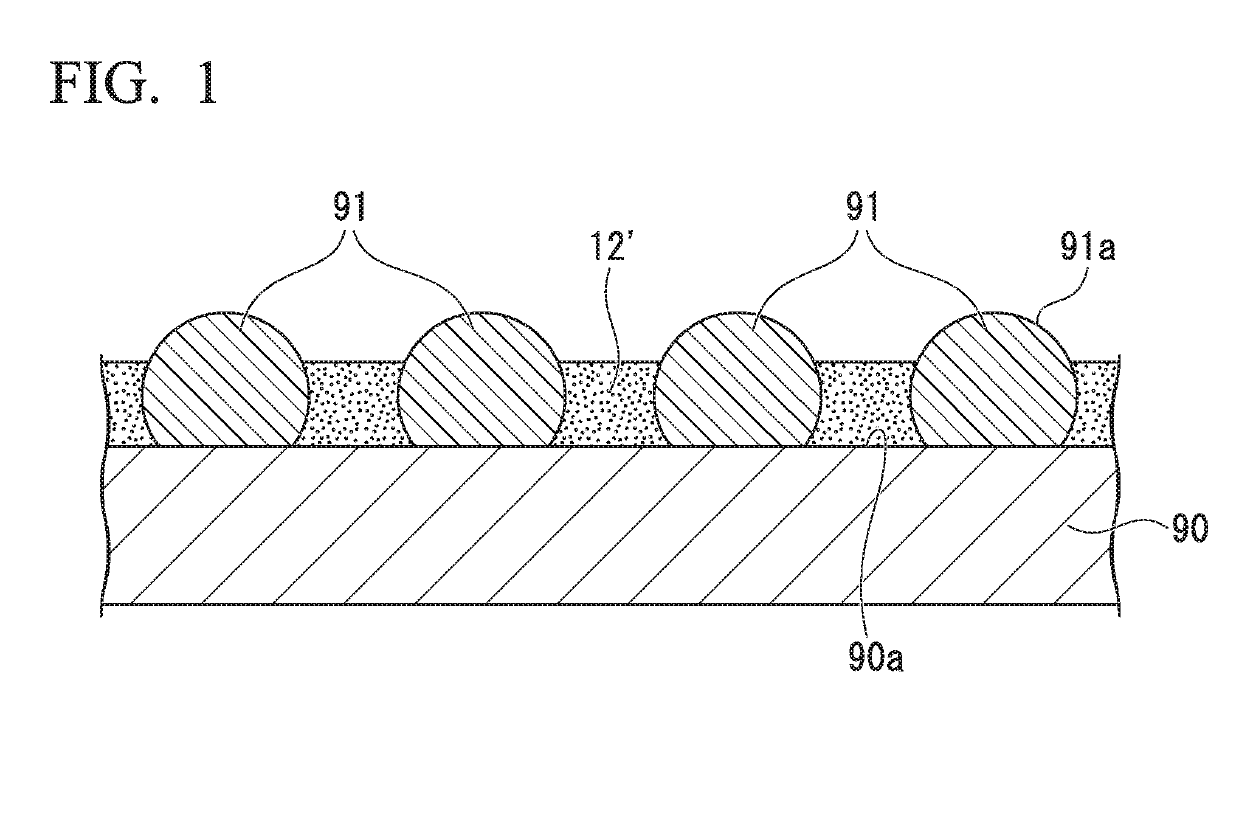
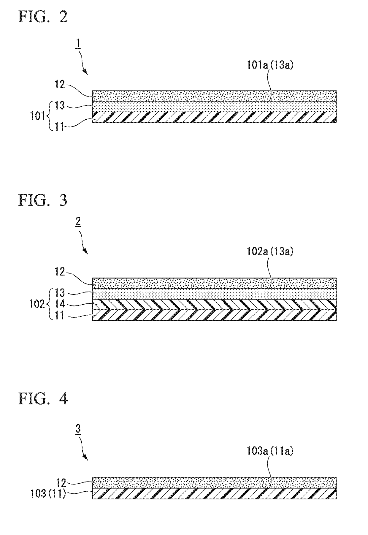
This curable resin film forms a first protective film on a surface having bumps of a semiconductor wafer by being attached to the surface and being cured, in which a cured material of the curable resin film has a Young's modulus of equal to or greater than 0.02 MPa and a peak value of a load measured by a probe tack test at 80° C. is equal to or less than 500 g. A first protective film forming sheet is provided with a first supporting sheet, and the curable resin film is provided on one surface of the first supporting sheet.

Description

CROSS REFERENCE TO RELATED APPLICATIONS[0001]This application is a continuation application of U.S. application Ser. No. 15 / 770,529, filed Apr. 24, 2018, which is the U.S. national phase of International Application No. PCT / JP2016 / 082539 filed Nov. 2, 2016 which designated the U.S. and claims priority to Japanese Patent Application No. 2015-217108, filed on Nov. 4, 2015, the entire contents of each of which are incorporated herein by reference.TECHNICAL FIELD[0002]The present invention relates to a curable resin film and a first protective film forming sheet using the same.[0003]Priority is claimed on Japanese Patent Application No. 2015-217108, filed on Nov. 4, 2015, the disclosure of which is incorporated herein by reference.BACKGROUND ART[0004]In the related art, in a case in which a multi-pin LSI package, which is used in MPU or a gate array, is mounted on a printed wiring board, a flip chip mounting method in which a semiconductor chip in which convex electrodes (bumps) made of...

Claims


Application Information

Patent Timeline
Patent Type & Authority Applications(United States)
IPC IPC(8): C08L63/00H01L23/00B32B7/02B32B27/30B32B27/32B32B27/36B32B27/38B32B27/08H01L23/12H01L21/56C09J7/38C08L33/08H01L21/78H01L23/29H01L23/31
CPCB32B27/308C08L2205/035C08L2205/025H01L23/293H01L21/56C09J7/385H01L2224/12105C08L63/00B32B27/32B32B2457/14B32B27/36H01L23/3171H01L24/12B32B27/38C08L33/08B32B7/02B32B2307/54B32B27/08H01L23/00H01L23/12H01L24/94H01L21/78H01L21/561H01L21/6835H01L2221/68327H01L2221/6834
Inventor SATO, AKINORIYAMAGISHI, MASANORI
Owner LINTEC CORP
Learn More