Method of mounting a multi-element matrix photodetector

a multi-element matrix and photodetector technology, applied in the direction of electrical equipment, basic electric elements, instruments, etc., can solve the problems of mechanical damage to silicon chips and failure of photoreceivers, and achieve the effects of facilitating the large movement of photoreceiver chips, reducing light loss, and high stability

Inactive Publication Date: 2019-11-07
OBSHCHESTVO S OGRANICHENNOJ OTVETSTVENNOSTJU NAUCHNO TEKHNICHESKIJ TSENTR MT OOO NTTS MT +1
View PDF1 Cites 0 Cited by
  • Summary
  • Abstract
  • Description
  • Claims
  • Application Information

AI Technical Summary

Benefits of technology

[0020]The liquid polymer applied to the surface of the FOP before the start of assembly, which cures further in the process, serves simultaneously for several purposes: it protects the surface of the photoreceivers from direct contact with the FOP; it implements optical immersion to minimize light loss at the edges of materials; it is the antifriction medium that facilitates greatly moving the photoreceiver chips relative to the FOP. Also the said polymer creates a durable adhesive interface between the FOP and the surface of the photoreceiver to form a highly stable structure, because the temperature coefficients of expansion of silicon and glass that make up the main material of the FOP are very close.
[0021]The scope is expanded due to the final fixation of the photoreceiver chips directly to the FOP and since the fiber-optic plate has the thermal expansion coefficient (TEC) comparable to that of silicon which is the material of the photoreceiver chip, the allowable temperature range of operation and storage of the manufactured product increases. In addition, the overall dimensions of the product are reduced, since the alignment elements are no longer needed to be left in the assembled structure.

Problems solved by technology

Such a collision can lead to mechanical damage to the silicon chips and the failure of photoreceivers.

Method used


Image

  • Method of mounting a multi-element matrix photodetector
  • Method of mounting a multi-element matrix photodetector
  • Method of mounting a multi-element matrix photodetector

Examples


Embodiment Construction

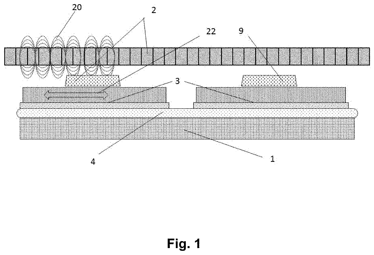
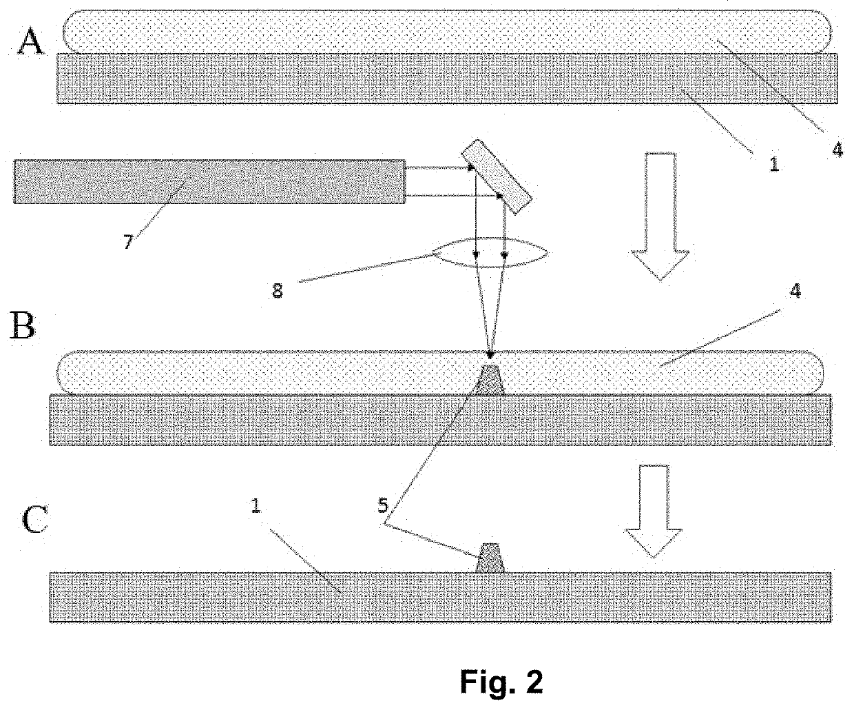
[0035]The matrix photodetector comprises at least one photoreceiver (3) located on the FOP (1) and fixed with the help of a polymerized (40) liquid optical polymer (4). Description of the method distinguishes the phases of the polymer when indicated by numbers on the figures. In the context of this description, N (4) states to indicate the liquid phase of the polymer, and N (40)—for the cured phase.

[0036]Initially, the liquid polymer is distributed over the FOP area evenly or partially, and then the photoreceiver or several photoreceivers are placed on the surface formed by the polymer. A partial distribution of a polymer is understood to be applied in the required volume on a part of the surface rather than the entire surface, usually in the shape of a drop, oval or dumbbell. In the case of partial distribution of the polymer on the FOP, the polymer spreads over the entire area of the FOP due to the compression forces and the capillary effect. At this stage, photoreceivers can be p...


PUM


Abstract

The proposed invention relates to the manufacturing of devices for detecting a visible or X-ray image or an image obtained when recording X-ray or gamma radiation, in particular devices for X-ray mammography and tomosynthesis. In a new method of mounting a multi-element matrix photodetector of visible or penetrating radiation, at least one matrix photoreceiver is positioned in a controllable manner by means of rotation and movement over the liquid phase of an optical polymer pre-applied to at least a part of a surface of a fiber-optic plate, and is subsequently fixed by curing of said polymer. In the process, there is no physical contact or touching of the surfaces of the photoreceiver and of the fiber-optic plate, which minimizes the probability of a photoreceiver chip being damaged.

Description

FIELD OF THE INVENTION[0001]The proposed invention relates to the manufacturing of devices for detecting a visible or X-ray image or an image obtained when recording X-ray or gamma radiation, in particular devices for X-ray mammography and tomosynthesis.BACKGROUND OF THE INVENTION[0002]To design digital matrix image sensors, X-ray detectors, including in mammography, the so-called “flat panel” photo sensors are used that record the visible radiation or the converted x-ray image (“shadow”) of the object under study. Such flat panel detectors are a full-size spatial (matrix) image sensor with a 1:1 conversion scale.[0003]The photodetector itself features high sensitivity in the visible wavelength range (400-700 nm), but it is generally insensitive to X-rays. Accordingly, scintillation screens (scintillators), which are based on phosphor coatings of various efficiencies and scattering characteristics, are used to convert the X-rays into visible light. Such a screen (scintillator) is ph...

Claims


Application Information

Patent Timeline
Patent Type & Authority Applications(United States)
IPC IPC(8): H01L31/18
CPCH01L31/18G02B6/4202G02B6/4249
Inventor SPORYSH, VLADIMIR IGOREVICHPUTILIN, ANDREI NIKOLAEVICHDABAGOV, ANATOLY RUDOLFOVICHBARINOV, ANATOLY ANDREEVICHSUPONNIKOV, DMITRY ALEXANDROVICH
Owner OBSHCHESTVO S OGRANICHENNOJ OTVETSTVENNOSTJU NAUCHNO TEKHNICHESKIJ TSENTR MT OOO NTTS MT
Why Eureka
Try Eureka