High Speed Handling of Ultra-Small Chips by Selective Laser Bonding and Debonding

a laser bonding and debonding technology, applied in metal working equipment, metal processing equipment, manufacturing tools, etc., can solve the problems of affecting the throughput and cost performance of the fan-out package, requiring hundreds of hours to get a reconstituted 12-inch wafer via pick-and-place processing, and affecting the speed of the process. , to achieve the effect of high speed handling

Active Publication Date: 2019-11-14
IBM CORP
View PDF0 Cites 11 Cited by
  • Summary
  • Abstract
  • Description
  • Claims
  • Application Information

AI Technical Summary

Benefits of technology

[0007]The present invention provides techniques for high speed handling of ultra-small chips (e.g., micro-chips) by selective laser bonding and / or debonding technology in wafer-level processes. In one aspect of the invention, a method includes: providing a first wafer including chips (e.g., micro-chips) bonded to a surface thereof; contacting the first wafer with a second wafer, the second wafer including a substrate bonded to a surface thereof, wherein the contacting aligns individual chips with bonding sites on the substrate; and debonding the individual chips from the first wafer using a debonding laser having a small spot size of about 0.5 μm to about 100 μm, and ranges therebetween.

Problems solved by technology

However, with micro-chip components (e.g., chip size of only 10× micrometers (μm)), it can take hundreds of hours to get a reconstituted 12-inch wafer via pick-and-place processing.
Further, high placement accuracy is always desired in wafer reconstitution, which makes the process even slower.
Thus, the wafer reconstitution process for micro-chips is time-consuming, affecting the throughput and cost performance of the fan-out package.
However, due to the ultra-small sizes and reduced thicknesses of micro-chip components, it is a challenge to provision a suitable vacuum nozzle for reliable assembly.
Namely, once chips are less than 300 micrometers (μm), handling and stiction can become a problem due to the gravitational force as compared to the surface forces.
Further, the down-force of the nozzle can easily crack thin chips during placement on the substrate.

Method used


Image

  • High Speed Handling of Ultra-Small Chips by Selective Laser Bonding and Debonding
  • High Speed Handling of Ultra-Small Chips by Selective Laser Bonding and Debonding
  • High Speed Handling of Ultra-Small Chips by Selective Laser Bonding and Debonding

Examples


Embodiment Construction

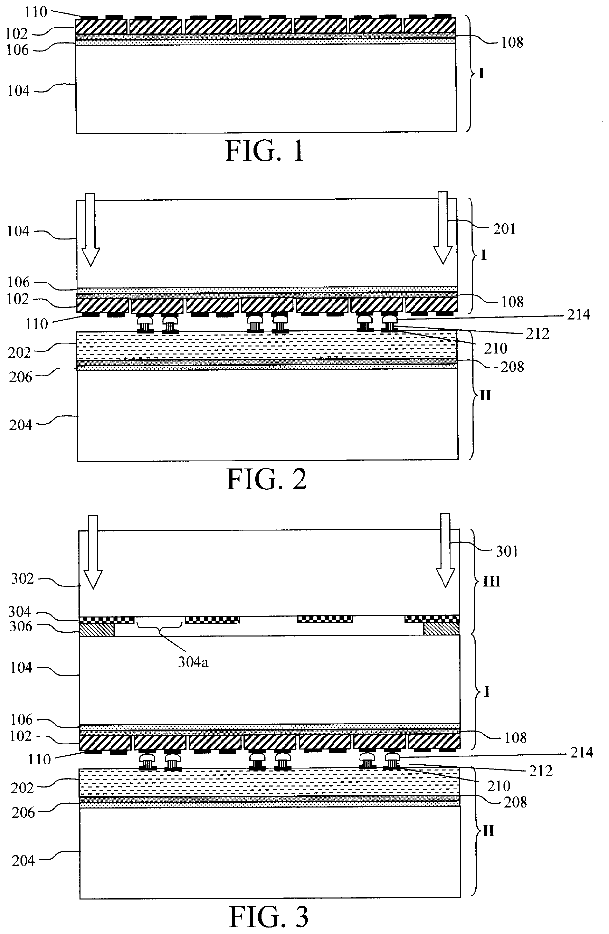
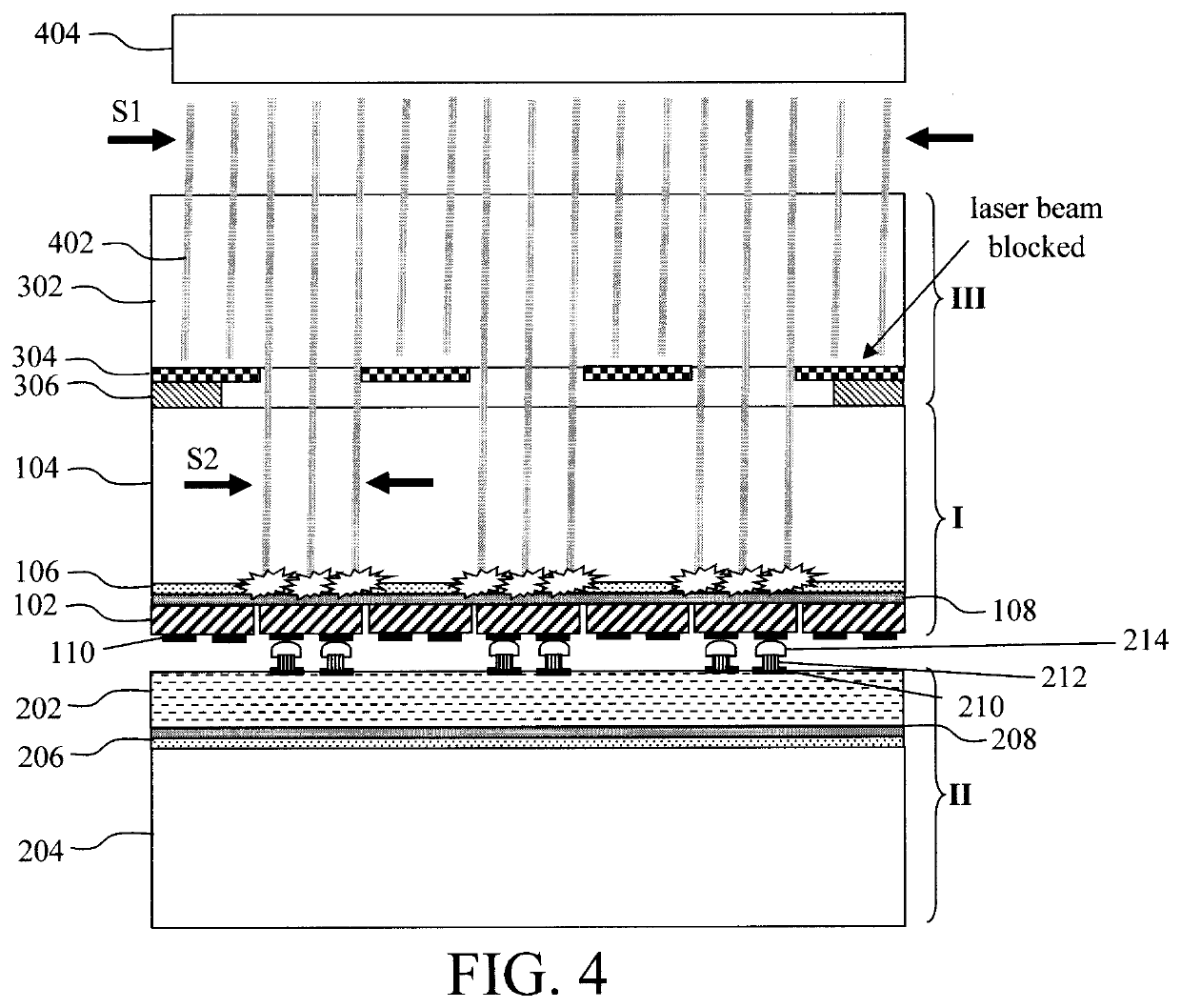
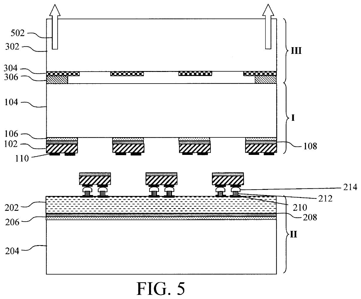
[0032]Provided herein are techniques for high-speed precision handling of micro-chips for fan-out wafer-level packaging (FOWLP) and other heterogeneous integration applications. The term “micro-chip,” as used herein, refers to a chip with a substrate that is less than 100 micrometers (μm)×100 μm. For instance, radio-frequency identification (RFID) chips typically have substrate dimensions of about 40 μm×40 μm, and light-emitting diode (LED) chips typically have substrate dimensions of about 8 μm×8 μm. Thus, RFID and LED chips are considered herein to be micro-chips.

[0033]As will be described in detail below, the present techniques employ a precise laser and optical guide system to selectively place micro-chips on a thin, flexible substrate from a handle wafer. In one exemplary embodiment, a template wafer is employed to focus a (large spot size) laser beam precisely onto specific locations on the handle wafer to release single micro-chips from the handle wafer. In another exemplary ...


PUM

PropertyMeasurementUnit
spot sizeaaaaaaaaaa
thicknessaaaaaaaaaa
thicknessaaaaaaaaaa

Abstract

Techniques for high speed handling of ultra-small chips (e.g., micro-chips) by selective laser bonding and/or debonding are provided. In one aspect, a method includes: providing a first wafer including chips bonded to a surface thereof; contacting the first wafer with a second wafer, the second wafer including a substrate bonded to a surface thereof, wherein the contacting aligns individual chips with bonding sites on the substrate; and debonding the individual chips from the first wafer using a debonding laser having a small spot size of about 0.5 μm to about 100 μm, and ranges therebetween. A system is also provided that has digital cameras, a motorized XYZ-axis stage, and a computer control system configured to i) control a spot size of the at least one laser source and ii) adjust a positioning of the sample to align individual chips with a target area of the laser.

Description

FIELD OF THE INVENTION[0001]The present invention relates to chip handling techniques, and more particularly, to high speed handling of ultra-small chips (e.g., micro-chips) by selective laser bonding and / or debonding.BACKGROUND OF THE INVENTION[0002]During fan-out wafer-level packaging (FOWLP), individual chips are precisely placed on a (reconstituted) thin wafer substrate. A mold is formed over the reconstituted wafer substrate, followed by a redistribution layer (RDL) and a solder layer.[0003]Pick-and-place machines operate by placing electronic components (such as chips, capacitors, resistors, etc.) sequentially, one after another, onto a substrate. With high-speed auto alignment and positioning equipment, a pick-and-place machine can efficiently achieve reconstituted wafers with chip sizes of 10× millimeters (mm) in minutes. However, with micro-chip components (e.g., chip size of only 10× micrometers (μm)), it can take hundreds of hours to get a reconstituted 12-inch wafer via ...

Claims


Application Information

Patent Timeline
Patent Type & Authority Applications(United States)
IPC IPC(8): H01L23/00H01L21/683H01L25/00
CPCH01L2224/95001H01L2924/1421H01L25/50H01L2924/12041H01L24/75H01L2224/95148H01L2224/75261H01L2224/75901H01L2224/8116H01L2224/81005H01L2224/81224H01L21/6835H01L2224/7598H01L2224/81132H01L24/95H01L24/98H01L2224/7999H01L2221/68322H01L2224/75804H01L2221/68381H01L24/799H01L2224/98H01L24/81H01L2224/75753H01L2224/81815H01L2224/95121H01L2221/68354H01L2224/16225H01L2224/81192H01L2224/81001H01L24/13H01L24/05H01L2924/181H01L24/94H01L2224/75801H01L2224/75263H01L2224/759H01L2224/75702H01L2224/75701H01L2224/75262B23K1/0056B23K1/018B23K1/0016B23K2101/42H01L2224/95136H01L2224/13147H01L2224/13111H01L2224/05599H01L2224/13155H01L2924/013H01L2924/01029H01L2924/0105H01L2924/00014H01L2924/01028
Inventor CHEN, QIANWENDANG, BINGBUDD, RUSSELLWEN, BOHUNG, LI-WENNAH, JAE-WOONGKNICKERBOCKER, JOHN
Owner IBM CORP
Why Eureka
Try Eureka