Exposure apparatus

a technology of exposure apparatus and exposure chamber, which is applied in the direction of microlithography exposure apparatus, photomechanical treatment, instruments, etc., can solve the problems of deteriorating throughput performance of exposure apparatus, long measurement time, and deteriorating overall productivity, so as to reduce production cost per ic, improve throughput and/or uptime, and improve overall productivity of lithographic apparatus

Active Publication Date: 2019-12-12
ASML NETHERLANDS BV
View PDF3 Cites 4 Cited by
  • Summary
  • Abstract
  • Description
  • Claims
  • Application Information

AI Technical Summary

Benefits of technology

[0006]Despite the exposure process is interrupted only briefly, there is a desire to expose substrates to create IC's with a further reduced production cost per IC. In general, overall productivity of a lithographic apparatus is improved when throughput and / or uptime is improved. Good imaging quality of a pattern transferred onto a substrate is often required for manufacturing ICs. More accurate measurement of a substrate enables better imaging quality; however, if a more accurate measurement of a substrate is achieved by making a measurement time longer, the longer measurement time will deteriorate the overall productivity. In other words, there can be a trade-off between the overall productivity and the imaging quality in known lithographic apparatuses.

Problems solved by technology

More accurate measurement of a substrate enables better imaging quality; however, if a more accurate measurement of a substrate is achieved by making a measurement time longer, the longer measurement time will deteriorate the overall productivity.
In general, in an exposure apparatus that comprises a single wafer stage, the time spent (prior to exposure) on the wafer alignment operation is a pure overhead time and directly deteriorates the throughput performance of the exposure apparatus.
Even in an exposure apparatus that comprises two wafer stages and a single wafer alignment system, in the case that the time spent on the wafer alignment operation is longer than the time spent on exposure, the throughput performance will be deteriorated.

Method used


Image

  • Exposure apparatus
  • Exposure apparatus
  • Exposure apparatus

Examples


Embodiment Construction

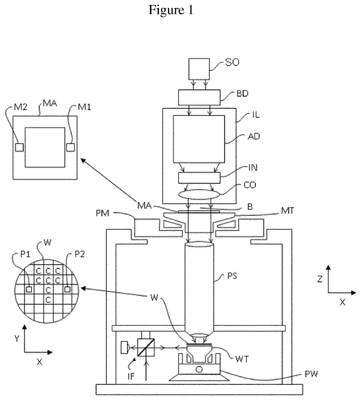
[0029]FIG. 1 schematically depicts a lithographic apparatus according to one embodiment of the invention. The lithographic apparatus comprises an illumination system IL, a support structure MT, a substrate table WT and a projection system PS. The illumination system IL is configured to condition a radiation beam B. The support structure MT is constructed to support a patterning device MA and is connected to a first positioning device PM configured to accurately position the patterning device MA in accordance with certain parameters. The substrate table WT is constructed to hold a substrate W, e.g., a resist-coated wafer, and is connected to a second positioner PW configured to accurately position the substrate W in accordance with certain parameters. The projection system PS is configured to project a pattern imparted to the radiation beam B by patterning device MA onto a target portion C (e.g. comprising one or more dies) of the substrate W.

[0030]The illumination system IL may incl...


PUM


Abstract

An exposure apparatus arranged to project a radiation beam onto a target portion of a substrate, the exposure apparatus having: a first substrate holder configured to hold the substrate; a second substrate holder configured to hold the substrate; a sensor holder configured to hold a sensor and / or detector; a first measurement device having a first alignment system having an alignment sensor configured to measure positions of a substrate alignment mark on the substrate; a second measurement device having a second alignment system having a further alignment sensor configured to measure positions of the substrate alignment mark on the substrate; a first scale arranged on a lower surface of the first substrate holder; and a first encoder head arranged to cooperate with the first scale, the first encoder head located beneath the first alignment system and held by a stationary support.

Description

CROSS REFERENCE TO RELATED APPLICATIONS[0001]This application claims priority of 1.EP application 17154551.0 which was filed on 2017 Feb. 3, claims priority of 2.EP application 17169025.8 which was filed on 2017 May 2, claims priority of 3.EP application 17193990.3 which was filed on 2017 Sep. 29, claims priority of 4.EP application 17201092.8 which was riled on 2017 Nov. 10 and which are incorporated herein in their entirety by reference.FIELD OF THE INVENTION[0002]The present invention relates to an exposure apparatus.BACKGROUND ART[0003]A lithographic apparatus is a machine that applies a desired pattern onto a substrate, usually onto a target portion of the substrate. A lithographic apparatus can be used, for example, in the manufacture of integrated circuits (ICs). In that instance, a patterning device, which is alternatively referred to as a mask or a reticle, may be used to generate a circuit pattern to be formed on an individual layer of the IC. This pattern can be transferr...

Claims


Application Information

Patent Timeline
Patent Type & Authority Applications(United States)
IPC IPC(8): G03F7/20
CPCG03F7/70491G03F7/70341G03F7/706G03F7/705G03F9/7046G03F7/201
Inventor KANEHARA, JUNICHI
Owner ASML NETHERLANDS BV
Why Eureka
Try Eureka