Integrated circuits employing varied gate topography between an active gate region(s) and a field gate region(s) in a gate(s) for reduced gate layout parasitic capacitance, and related methods

a technology of integrated circuits and gate topography, which is applied in the field of integrated circuits, can solve the problems of increasing the parasitic capacitance of field gates, and achieve the effects of reducing the overall volume of gate materials, and reducing gate layout parasitic capacitan

Inactive Publication Date: 2020-01-16
QUALCOMM INC
View PDF4 Cites 9 Cited by
  • Summary
  • Abstract
  • Description
  • Claims
  • Application Information

AI Technical Summary

Benefits of technology

[0008]Aspects disclosed herein include integrated circuits employing varied gate topography between an active gate region(s) and a field gate region(s) in a gate(s) for reduced gate layout parasitic capacitance. Related methods are also disclosed. For example, an integrated circuit may include one or more Field-Effect Transistors (FETs), such as a planar FET, a FinFET, and / or a gate-all-around (GAA) (e.g., nanowire, nanoslab, or nanosheet) FET. In exemplary aspects disclosed herein, the gate topography (e.g., height) of a gate in a circuit cell used to form gates for devices formed from the circuit cell is varied between an active region(s) of the gate (“active gate(s)”) and a field region(s) of the gate (“field gate(s)”). In this manner, the overall volume of material in the gate can be reduced due to the reduction in volume of the field gate(s) to reduce gate layout parasitic capacitance, while the volume of gate material in the active gate(s) can remain to provide the desired geometry to provide effective control of a channel of a FET and / or to not change the FET behavior. The gate layout parasitic capacitance occurs as a result of the gate located in close proximity to metal contacts and / or interconnects providing a parallel plate-like capacitance. Reducing gate layout parasitic capacitance in a circuit cell can reduce the overall parasitic capacitance of an integrated circuit formed from the circuit cell using the gate to form an active gate to achieve the desired delay performance in the integrated circuit.

Problems solved by technology

This is because removing Fins from the circuit cell can increase the field gate regions in the circuit cell, thus increasing the field gate parasitic capacitance.

Method used


Image

  • Integrated circuits employing varied gate topography between an active gate region(s) and a field gate region(s) in a gate(s) for reduced gate layout parasitic capacitance, and related methods
  • Integrated circuits employing varied gate topography between an active gate region(s) and a field gate region(s) in a gate(s) for reduced gate layout parasitic capacitance, and related methods
  • Integrated circuits employing varied gate topography between an active gate region(s) and a field gate region(s) in a gate(s) for reduced gate layout parasitic capacitance, and related methods

Examples


Embodiment Construction

[0039]With reference now to the drawing figures, several exemplary aspects of the present disclosure are described. The word “exemplary” is used herein to mean “serving as an example, instance, or illustration.” Any aspect described herein as “exemplary” is not necessarily to be construed as preferred or advantageous over other aspects.

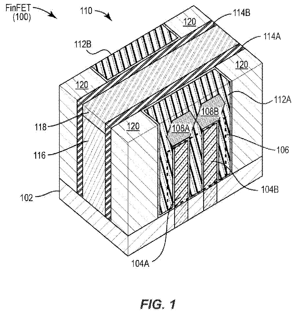
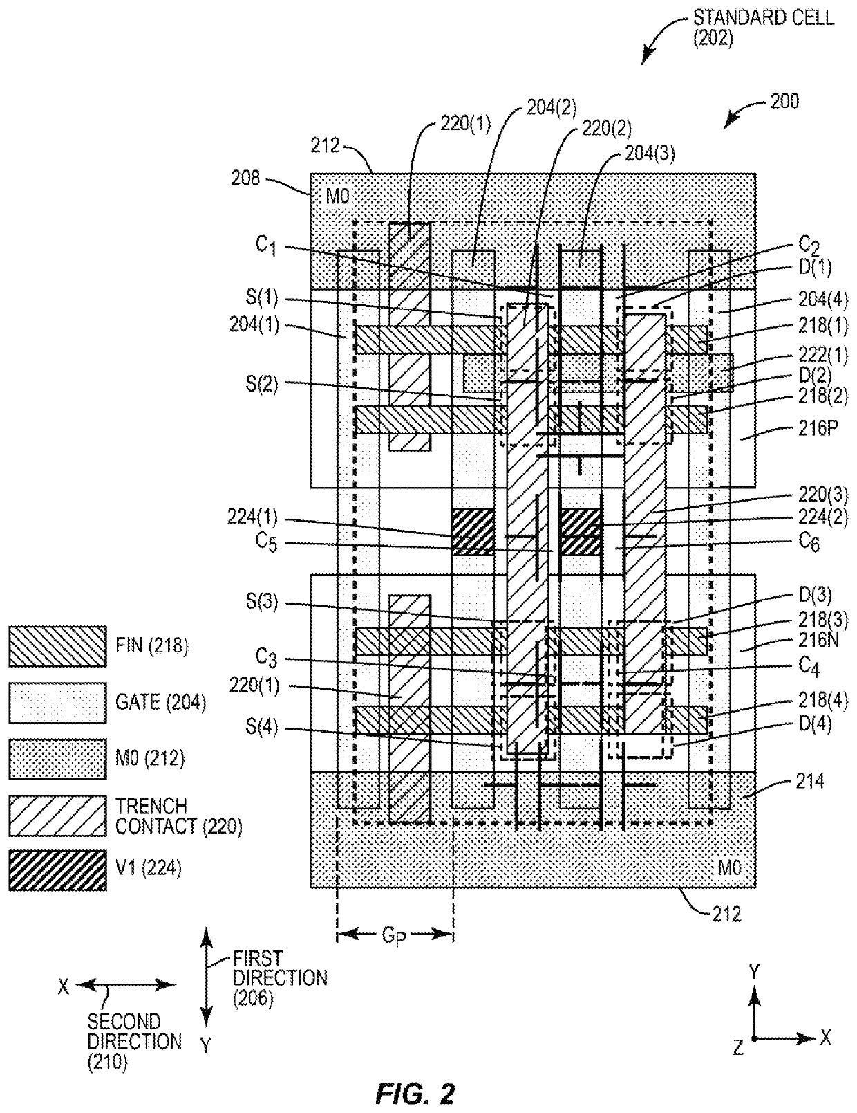
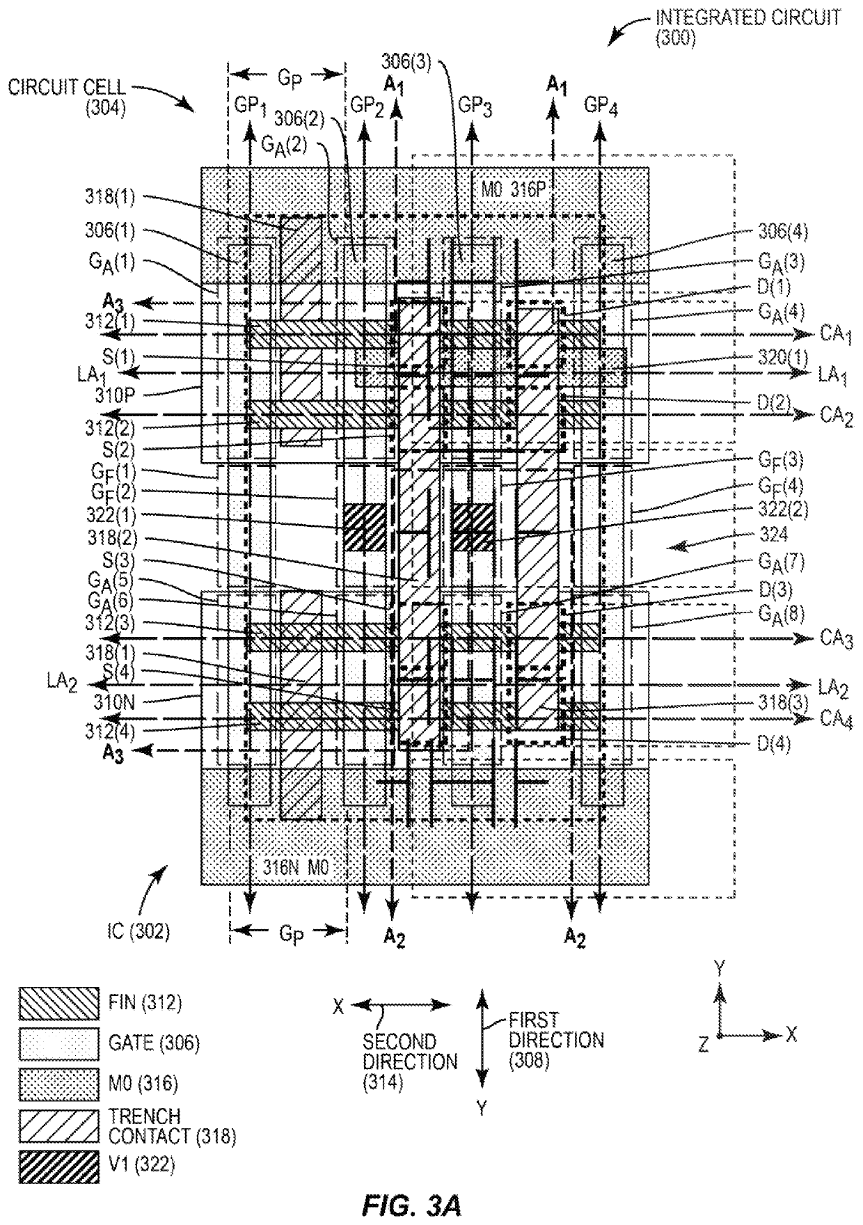
[0040]Aspects disclosed herein include integrated circuits employing varied gate topography between an active gate region(s) and a field gate region(s) in a gate(s) for reduced gate layout parasitic capacitance. Related methods are also disclosed. For example, an integrated circuit may include one or more Field-Effect Transistors (FETs), such as a planar FET, a FinFET, and / or a gate-all-around (GAA) (e.g., nanowire, nanoslab, or nanosheet) FET. In exemplary aspects disclosed herein, the gate topography (e.g., height) of a gate in a circuit cell used to form gates for devices formed from the circuit cell is varied between an active region(s) of the gat...


PUM

PropertyMeasurementUnit
areaaaaaaaaaaa
height HAaaaaaaaaaa
height HFaaaaaaaaaa

Abstract

Integrated circuits employing varied gate topography between an active gate region(s) and a field gate region(s) in a gate(s) for reduced gate layout parasitic capacitance, and related methods, are disclosed. In exemplary aspects, the gate topography (e.g., height) of a gate in a circuit cell used to form gates for devices formed therein to form an integrated circuit is varied between an active gate and a field gate(s) of the gate. In this manner, the overall volume of material in the gate can be reduced due to the reduction in volume of the field gate(s) to reduce gate layout parasitic capacitance. Reducing gate layout parasitic capacitance in a circuit cell can reduce the overall parasitic capacitance of an integrated circuit formed from the circuit cell to achieve the desired integrated circuit delay performance.

Description

BACKGROUNDI. Field of the Disclosure[0001]The technology of the disclosure relates generally to integrated circuits, such as planar transistors, Fin Field-Effect Transistors (FETs) (FinFETs), and gate-all-around (GAA) transistors, formed from a circuit cell, such as a complementary metal-oxide semiconductor (CMOS) standard cell, in integrated circuits (ICs).II. Background[0002]Transistors are essential components in modern electronic devices, and large numbers of transistors are employed in integrated circuits (ICs) therein. For example, components such as central processing units (CPUs) and memory systems each employ a large quantity of transistors for logic circuits and memory devices. For example, FIG. 1 illustrates a conventional complementary metal-oxide semiconductor (CMOS) Fin Field-Effect Transistor (FET) 100 (“FinFET 100”) as an example of a transistor. A FinFET includes a gate material wrapped around at least a portion of a channel structure to provide better gate control ...

Claims


Application Information

Patent Timeline
Patent Type & Authority Applications(United States)
IPC IPC(8): H01L27/088H01L29/08H01L29/10H01L29/423H01L29/40H01L21/8234H01L29/66H01L21/027H01L21/3213H01L27/02
CPCH01L27/0207H01L27/0886H01L29/0847H01L21/823437H01L21/823431H01L29/42376H01L21/0273H01L29/42392H01L21/823807H01L21/823828H01L21/823412H01L21/823821H01L29/66545H01L21/32139H01L27/0924H01L29/1037H01L29/402H01L21/82385H01L29/0673H01L29/41791H01L29/775H01L2027/11874
Inventor BADAROGLU, MUSTAFARIM, KERN
Owner QUALCOMM INC
Why Eureka
Try Eureka