

Manufacturing method of quantum dot structure
- Summary
- Abstract
- Description
- Claims
- Application Information
AI Technical Summary
Benefits of technology
Problems solved by technology
Method used
Image

Examples
embodiment 1
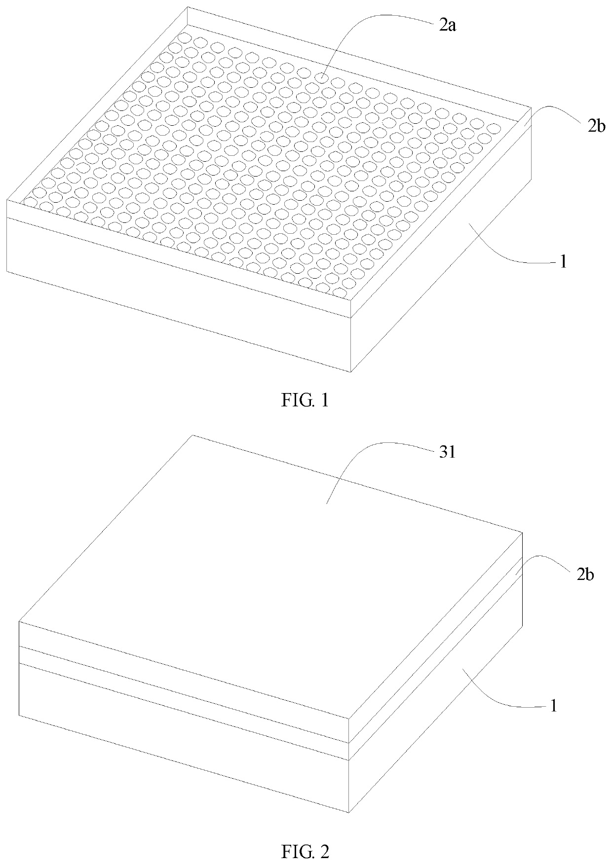
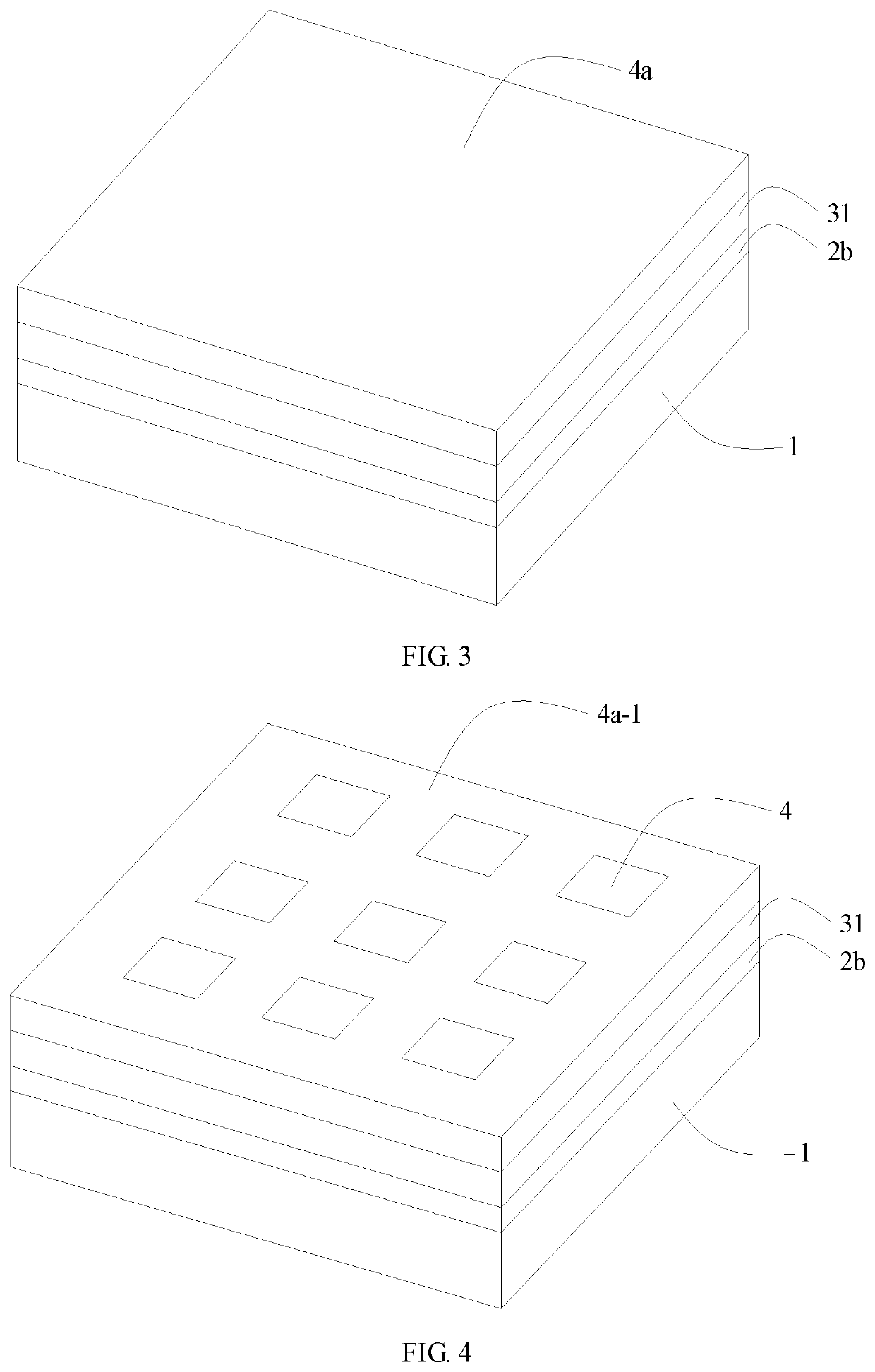
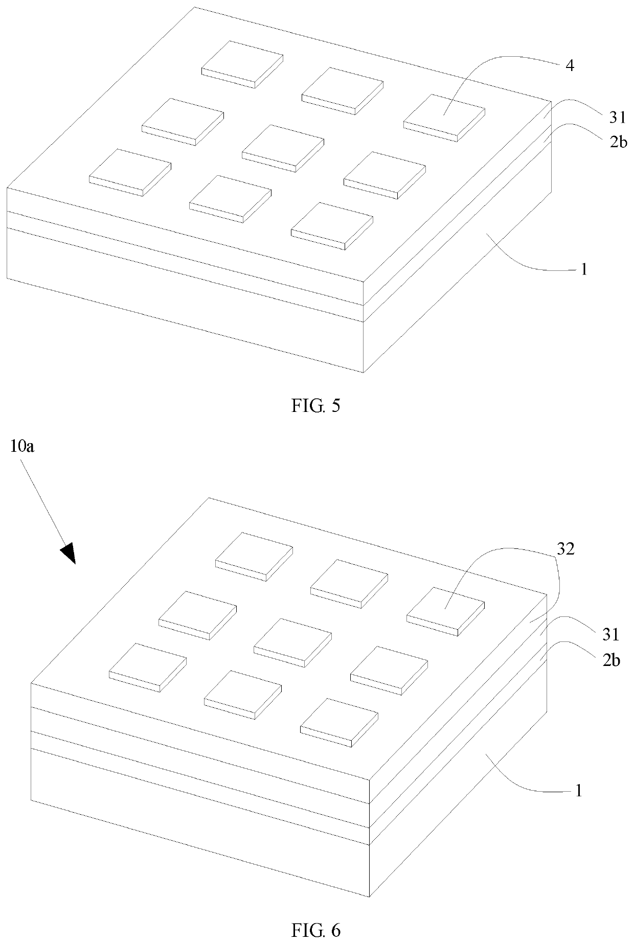
[0027]FIGS. 1-7 are process flow charts of a manufacturing method of a quantum dot structure according to the present embodiment.
[0028]Referring to FIGS. 1-7 for details, the manufacturing method of the quantum dot structure according to the present embodiment includes the following steps:
[0029]Step 1: providing a quantum dot film layer 2a on a substrate 1.
[0030]In specific, in the present embodiment, a material of the substrate 1 is GaAs; a material of the quantum dot film layer 2a is InAs; a thickness of the quantum dot film layer 2a is 1.4 ML˜10 ML, preferably is 1.4 ML˜5 ML; and a density of quantum dots in the quantum dot film layer 2a is 108 cm−2˜1011 cm−2. Here, ML is a monolayer, and is also a thickness of the monolayer.
[0031]More particularly, the quantum dot film layer 2a is grown by adopting a molecular beam epitaxy SK mode, and a growing temperature is 300° C. ˜550° C.; and the specific process of providing the quantum dot film layer 2a by adopting the molecular beam epi...
embodiment 2
[0046]In the description of Embodiment 2, the same point with Embodiment 1 is no longer stated herein, and differences with Embodiment 1 are only described. The manufacturing method of the quantum dot structure in Embodiment 2 differs from that in Embodiment 1 in that specific methods of providing the patterned array 4 on the first protection film 31 in Step 3 are different.
[0047]Referring to FIGS. 8-10, the present embodiment manufactures the patterned array 4 on the first protection film 31 by adopting a photolithography process.
[0048]Specifically, the following steps are referred to: (1) spin coating a photoresist layer 4b on the first protection film 31 by using a photoresist spinner, as shown in FIG. 8; (2) performing a patterning process on the photoresist layer 4b by adopting a photolithography process, the photoresist layer 4b forming a photolithography adhesive residue 4b-2, meanwhile, a concave hole 4b-1 matching a shape of a pre-manufactured patterned array 4 being formed...
embodiment 3
[0052]In the description of Embodiment 3, the same point with Embodiment 2 is no longer stated herein, and differences from Embodiment 2 are only described. The manufacturing method of the quantum dot structure in Embodiment 3 differs from that in Embodiment 2 in that specific methods of providing the patterned array on the first protection film in Step 3 are different. Meanwhile, the annealing time and the annealing temperature for annealing the intermediate body in Step 5 are different.
[0053]Specifically, the present embodiment replaces the photolithography process of step (2) of Step 3 in Embodiment 2 with the electron beam photolithography process so as to perform a patterning process on the photoresist layer.
[0054]It is worth noting that, in view of controlling precise of the electron beam photolithography process, a characteristic size of the finally obtained patterned array is 10 nm˜200 μm, that is, a length and / or width of the obtained patterned array is 10 nm˜200 nm.
[0055]I...
PUM
 Abstract
Description
Claims
Application Information