Resin encapsulated power semiconductor module with exposed terminal areas

a technology of power semiconductor modules and exposed terminals, which is applied in the direction of semiconductor devices, semiconductor device details, semiconductor/solid-state device details, etc., can solve the problems of further module size reduction, limit the freedom regarding the design of the terminal and the substrate, and limit the freedom of the transfer-molded power semiconductor module with leadframe terminals. , to achieve the effect of improving electrical performance, reducing the size of the module, and increasing the freedom of the substrate and the terminal design

Active Publication Date: 2020-02-27
HITACHI ENERGY SWITZERLAND AG +1
View PDF0 Cites 7 Cited by
  • Summary
  • Abstract
  • Description
  • Claims
  • Application Information

AI Technical Summary

Benefits of technology

[0030]The power semiconductor module may have an improved electrical performance, due to more freedom regarding substrate and terminal design. Terminal positions are not restricted by requirements imposed by a leadframe in combination with a transfer molding approach. For example, a shorter connection to a DC link capacitor may be provided, since no space for a busbar to terminal welding is needed. A shorter connection may lead to a lower commutation loop inductance. Additionally, shorter auxiliary connections may lead to a reduced gate inductance.
[0031]A manufacturing and mounting of the power semiconductor module may result in reduced costs, since terminals and terminal attachment processes are not needed anymore. For example, there may be an improved flexibility regarding terminal connections. In different applications, different connection technologies may be used. A direct welding of busbars to the terminal areas at least does not require more effort than a welding of busbars to terminals.
[0032]The power semiconductor module may have an improved manufacturability. The one or more power semiconductor chips may be protected from particle contamination during an ultrasonic welding process of a conductor to a terminal area, which may be performed after the molding. Also, the molding process may be simplified and risks due to difficult sealing of multiple leadframes with different thicknesses are avoided.

Problems solved by technology

This may result in several limitations for a transfer-molded power semiconductor module with leadframe terminals.
This may limit the freedom regarding the terminal and substrate design, and may also prohibit a further size reduction of the module, in case many terminals are needed.
Furthermore, using multiple leadframes of different thicknesses and / or materials may be challenging regarding a sealing of the mold.
Terminals sticking out at the side of a power semiconductor module may impose limitations on an attachment of the module to a cooler: Access to the interface between baseplate and cooler may be needed from the top, which may be obstructed by the leadframe terminals.

Method used


Image

  • Resin encapsulated power semiconductor module with exposed terminal areas
  • Resin encapsulated power semiconductor module with exposed terminal areas
  • Resin encapsulated power semiconductor module with exposed terminal areas

Examples


Embodiment Construction

[0016]It is an objective of the invention to provide an easy to manufacture and easy to assembly power semiconductor module and / or to provide a power semiconductor module with electrical connections having a low stray inductance.

[0017]These objectives arc achieved by the subject-matter of the independent claims. Further exemplary embodiments are evident from the dependent claims and the following description.

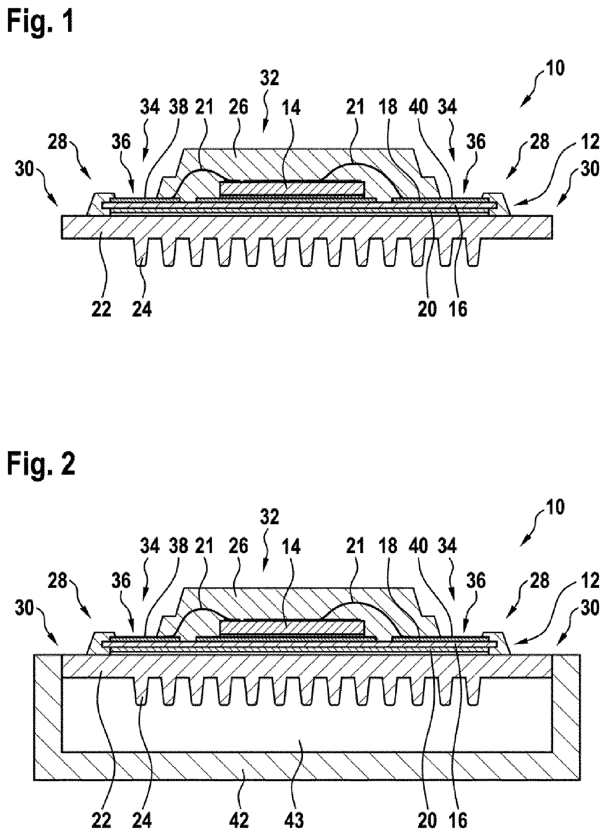
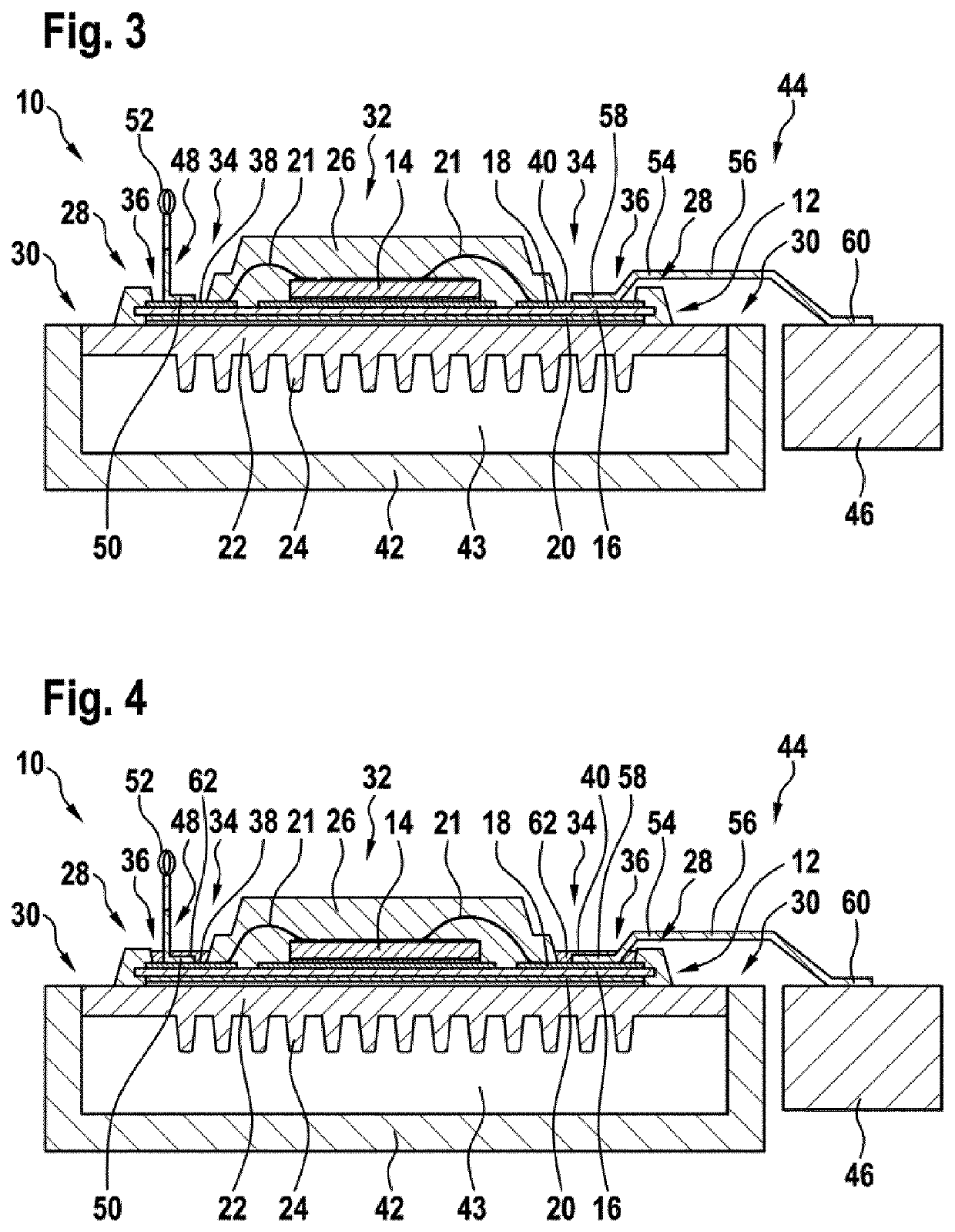
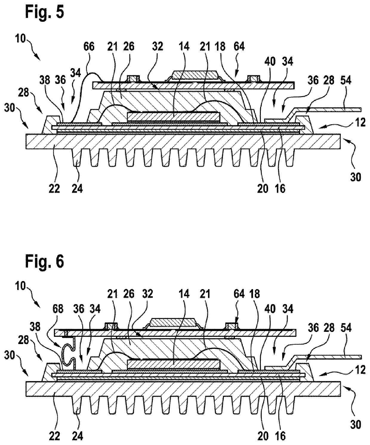
[0018]A first aspect of the invention relates to a power semiconductor module. A semiconductor module may be any device composed of one or more semiconductor chips, their electrical and mechanical interconnections and a housing for these components. The term “power” here and in the following may refer to modules and / or semiconductor chips adapted for processing current of more than 100 V and / or more than 10 A. For example, the power semiconductor module may be used in automotive applications, such as electric vehicles, hybrid vehicles, motorbikes, busses, trucks, off-road constr...


PUM

PropertyMeasurementUnit
current ratingaaaaaaaaaa
voltage ratingaaaaaaaaaa
currentaaaaaaaaaa

Abstract

A power semiconductor module includes a substrate with a metallization layer; at least one power semiconductor chip bonded to the substrate; and a mold encapsulation partially encapsulating the semiconductor chip and the substrate; the mold encapsulation includes at least one window exposing a terminal area of the metallization layer; and a border part of the mold encapsulation between the window and a border of the substrate has a height over the substrate smaller than a maximal height of a central part of the mold encapsulation.

Description

FIELD OF THE INVENTION[0001]The invention relates to a power semiconductor module, a power semiconductor module assembly and a method for manufacturing a power semiconductor module.BACKGROUND OF THE INVENTION[0002]Power semiconductor modules containing solid-state semiconductor switches, such as IGBTs or MOSFETs, arc used in various power electronics applications to switch or rectify electric currents. An important and fast growing application are converter systems for electric or hybrid electric vehicles. A typical module for such applications may have a voltage rating of up to 1200 V and a current rating of several hundred amperes.[0003]Usually, a power semiconductor module requires multiple electrical terminals, by which the DC and AC load currents are connected to an external busbar. Auxiliary signal terminals, such as for controlling the gates of the semiconductor chips in the module, are connected to an external gate driver circuit board.[0004]The power terminals are preferabl...

Claims


Application Information

Patent Timeline
Patent Type & Authority Applications(United States)
IPC IPC(8): H01L23/31H01L23/367H01L21/56H01L21/48H01L23/00H01L25/16H01L23/498
CPCH01L23/3121H01L21/565H01L21/4853H01L2224/48106H01L23/49861H01L2924/19107H01L2924/30107H01L23/3675H01L24/48H01L25/162H01L2224/48227H01L2224/48091H01L23/473H01L2924/181H01L2924/1815H01L2924/00014H01L2924/1301H01L24/32H01L24/73H01L2224/32225H01L2224/73265H01L2924/10253H01L2924/10272H01L2924/1203H01L2924/13055H01L2924/13091H01L23/3735H01L23/4334H01L2924/00012H01L2224/45099
Inventor MOHN, FABIAN
Owner HITACHI ENERGY SWITZERLAND AG
Why Eureka
Try Eureka