Conductive bridge semiconductor component and manufacturing method therefor

a technology of semiconductor components and semiconductor components, applied in the field of memory technology, can solve the problems of insufficient operating voltage, inability to store data, and inability to meet the requirements of the storage state, and achieve the effect of improving the retention characteristics of the resistive state, facilitating the concentrated distribution of conductive paths, and precise control of the ion barrier layer

Active Publication Date: 2020-02-27
INST OF MICROELECTRONICS CHINESE ACAD OF SCI
View PDF0 Cites 4 Cited by
  • Summary
  • Abstract
  • Description
  • Claims
  • Application Information

AI Technical Summary

Benefits of technology

[0020]It can be seen from the above technical solutions that the conductive bridge semiconductor device of the present disclosure and the method of manufacturing the same have at least one of the following advantageous effects:
[0021](1) By introducing a hole-containing ion barrier layer, there is provided a novel conductive bridge semiconductor device structure including an active upper electrode / ion barrier layer containing hole(s) / resistive switching functional layer / lower electrode;
[0022](2) Precise control of the ion barrier layer with different hole types, the quantity, size and density of the conductive filaments in the conductive bridge memory and selector can be well modulated;
[0023](3) For the conductive bridge resistive random access memory, a single nano-scale hole may facilitate the concentrated distribution of the conductive paths, improve the retention characteristics of the resistive state, and realize the non-volatile resistive switching characteristics under a small operating current, thereby effectively reducing the power consumption of the conductive bridge resistive random access memory;
[0024](4) For the conductive bridge selector, the array of holes in the ion barrier layer may facilitate the discrete distribution of the conductive paths, reduce the retention characteristics of the conductive paths, and realize the volatile resistive switching characteristics under the large operating current, thereby improving the drive current and selectivity ratio of the conductive bridge selector.

Problems solved by technology

With the continuous innovation of microelectronics and semiconductor technology, FLASH storage technology is facing a series of bottlenecks, for example, floating gates cannot be unrestricted thinning with the development of technology, data retention time is limited, operating voltage is too large and so on.
However, the random formation of the conductive path of the non-volatile resistive random access memory greatly impairs the memory characteristics of the conductive bridge resistive random access memory, that is, the retention characteristics of the resistive state, and is not facilitated to the low power consumption characteristics of the device under low current limit.
At the same time, the cross array architecture based resistive random access memory has a problem of crosstalk in the read operation in the array, resulting in erroneous reading of the stored information.
This type of selector usually has a slowly changing electrical characteristic and a small selectivity ratio, and cannot provide a high operating current to the resistive random access memory.
However, when this type of selector operates at a large operating current, the retention characteristics of the conductive bridge change, become not easily broken and become a non-volatile storage characteristic, and thus cannot perform strobing of the device.

Method used


Image

  • Conductive bridge semiconductor component and manufacturing method therefor
  • Conductive bridge semiconductor component and manufacturing method therefor
  • Conductive bridge semiconductor component and manufacturing method therefor

Examples


first embodiment

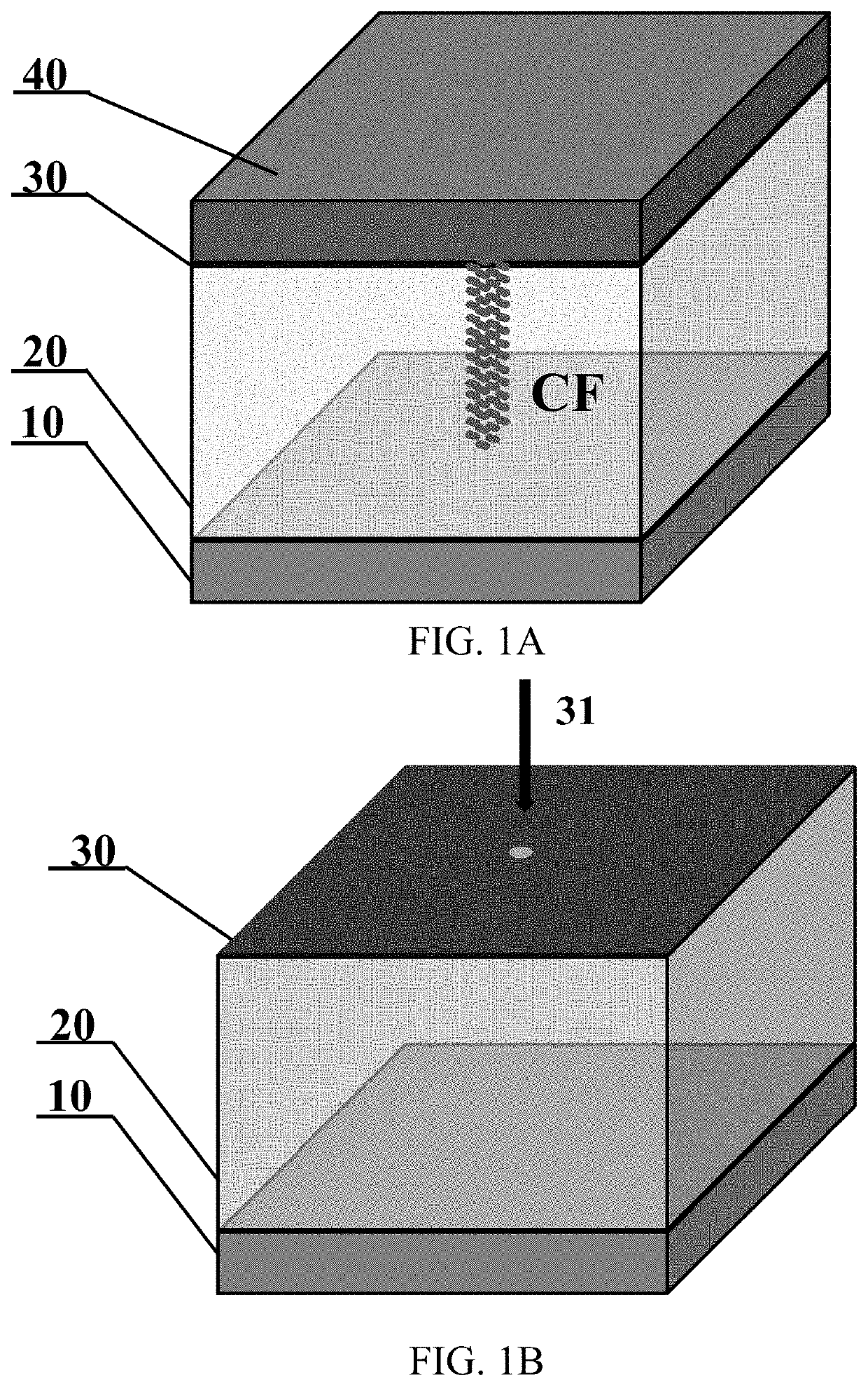
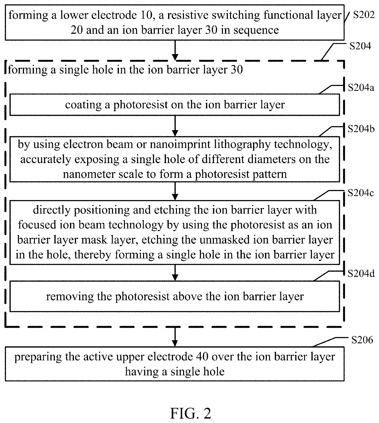
[0046]In a first exemplary embodiment of the present disclosure, a conductive bridge resistive random access memory is provided. FIG. 1A is a schematic view showing the structure and conductive path regulation of a conductive bridge resistive random access memory with a single hole in an ion barrier layer according to the present disclosure. FIG. 1B is a schematic diagram of the single hole in the ion barrier layer of the conductive bridge resistive random access memory shown in FIG. 1A. As shown in FIG. 1A and FIG. 1B, the conductive bridge resistive random access memory includes sequentially a lower electrode 10, a resistive switching functional layer 20, an ion barrier layer 30 and an active upper electrode 40 from bottom to top. Wherein, the ion barrier layer is provided with a single hole 31 through which the active conductive ions pass.

[0047]The respective portions of the conductive bridge resistive random access memory of the present embodiment are described in detail below.

[...

second embodiment

[0085]So far, the conductive bridge selector in the present disclosure has been described.

[0086]It will be apparent to those skilled in the art that in addition to the conductive bridge resistive random access memory and the conductive bridge selector, other semiconductor devices employing the conductive bridge principle are still applicable to the present disclosure and will not be described herein.

[0087]It should be noted that the implementations that are not shown or described in the drawings or the text of the specification are all known to those of ordinary skill in the art and are not described in detail. In addition, the above definitions of the various elements and methods are not limited to the specific structures, shapes, dimensions or manners mentioned in the embodiments, and those skilled in the art can simply modify or replace them, for example:

[0088](1) The lower electrode may also be in the form of a conductive oxide such as ITO;

[0089](2) The resistive switching funct...


PUM

PropertyMeasurementUnit
radial sizeaaaaaaaaaa

Abstract

The present disclosure provides a conductive bridge semiconductor device and a method of manufacturing the same. The conductive bridge semiconductor device includes a lower electrode, a resistive switching functional layer, an ion barrier layer and an active upper electrode from bottom to top, wherein the ion barrier layer is provided with certain holes through which active conductive ions pass. Based on this structure, the precise designing of the holes on the barrier layer facilitates the modulation of the quantity, size and density of the conduction paths in the conductive bridge semiconductor device, which enables that the conductive bridge semiconductor device can be modulated to be a nonvolatile conductive bridge resistive random access memory or a volatile conductive bridge selector. Based on the above method, ultra-low power nonvolatile conductive bridge memory and high driving-current volatile conductive bridge selector with controllable polarity are completed.

Description

CROSS-REFERENCE TO RELATED APPLICATION[0001]This application is a US national phase application of the international application PCT / CN2017 / 075141, filed on Feb. 28, 2017, entitled “CONDUCTIVE BRIDGE SEMICONDUCTOR COMPENONT AND MANUFACTURING METHOD THEREFOR,” which is incorporated herein by reference in its entirety.TECHNICAL FIELD[0002]The present disclosure relates to the field of memory technology in the microelectronics industry, and in particular, to a conductive bridge semiconductor device and a method of manufacturing the same.BACKGROUND[0003]With the continuous innovation of microelectronics and semiconductor technology, FLASH storage technology is facing a series of bottlenecks, for example, floating gates cannot be unrestricted thinning with the development of technology, data retention time is limited, operating voltage is too large and so on. Among many new types of memories, a resistive random access memory has now become the research focus of the new non-volatile memor...

Claims


Application Information

Patent Timeline
Patent Type & Authority Applications(United States)
IPC IPC(8): H01L45/00
CPCH01L45/085H01L45/146H01L45/165H01L45/1233H01L45/1253H01L45/1246H01L29/06H10N70/245H10N70/828H10N70/011H10N70/826H10N70/8833H10B41/35H10N70/043H10N70/841
Inventor LIU, QIZHAO, XIAOLONGLIU, SENLIU, MINGLV, HANGBINGLONG, SHIBINGWANG, YANWU, FACAI
Owner INST OF MICROELECTRONICS CHINESE ACAD OF SCI
Why Eureka
Try Eureka