
Non-volatile memory and manufacturing method for the same

a manufacturing method and non-volatile memory technology, applied in the field of semiconductor devices, can solve the problems of large memory cell size, poor data retention, and other problems, and achieve the effects of reducing device size, preventing leakage current, and increasing the thickness of the tunneling dielectric layer

Active Publication Date: 2020-05-14
NEXCHIP SEMICON CO LTD
View PDF0 Cites 5 Cited by
  • Summary
  • Abstract
  • Description
  • Claims
  • Application Information

AI Technical Summary

Benefits of technology

The present invention provides a non-volatile memory with a split-gate structure that reduces device size and prevents current leakage, improving data retention. The memory has a floating gate structure with sharp portions that increase the thickness of the tunneling dielectric layer to prevent leakage current. During programming and erase operations, the sharp portions enhance the FN tunneling effect and improve erase efficiency, respectively.

Problems solved by technology

A thin tunneling dielectric layer easily causes current leakage, and electric charge stored in the floating gate will leak to the erasing gate and be erased, thereby causing poor data retention.
However, the technical solution in the U.S. Pat. No. 9,502,581B2 has another problem.
The design of two independent transistors causes a large memory cell size, which does not meet the requirement of miniaturizing memory cells.

Method used


Image

  • Non-volatile memory and manufacturing method for the same
  • Non-volatile memory and manufacturing method for the same
  • Non-volatile memory and manufacturing method for the same

Examples


Embodiment Construction

[0066]Implementations of the present invention are illustrated below through specific embodiments. Persons skilled in the art can easily understand other advantages and efficacy of the present invention according to the content disclosed in this specification. The present invention can also be implemented or applied through other different specific implementations. Various modifications or variations can also be made on details in this specification based on different opinions and applications without departing from the spirit of the present invention.

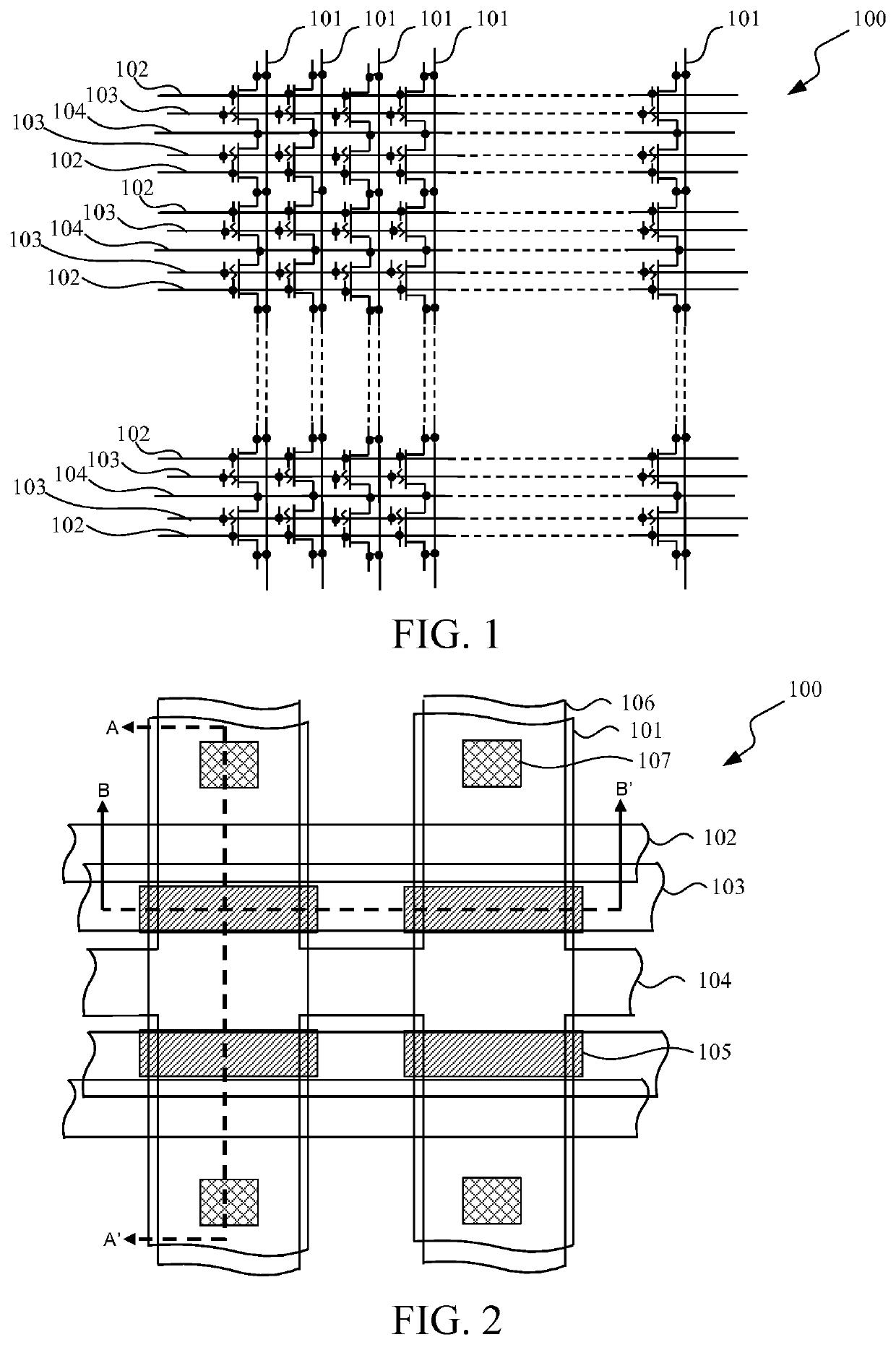
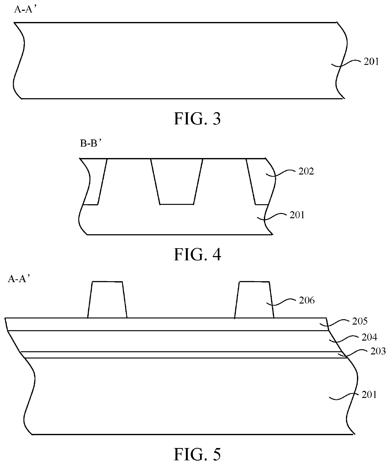
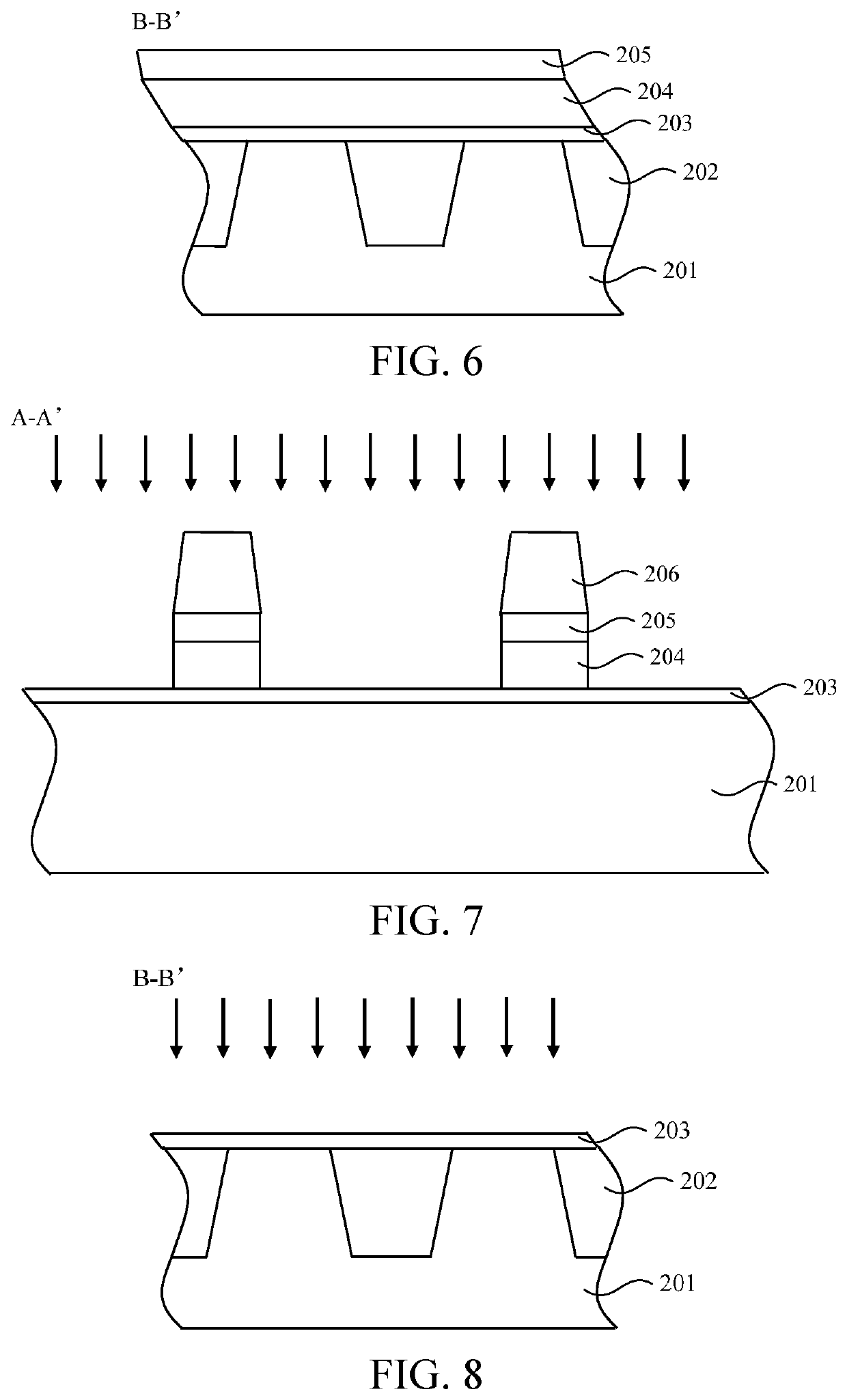
[0067]Refer to FIGS. 1 to 32. It should be noted that, the figures provided in this embodiment merely illustrate the basic conception of the present invention schematically. Therefore, the figures only show components related to the present invention, and are not drawn according to the quantity, shapes and sizes of components during actual implementation. The pattern, quantity and ratio of components during actual implementation can be...


PUM


Abstract

The present invention provides a non-volatile memory and a manufacturing method for the same. A floating gate structure of the non-volatile memory is located on one side of a word line structure, and includes a second gate dielectric layer and a second conductive layer in sequence from bottom to top. The second conductive layer has a first sharp portion, a second sharp portion, and a sharp depression portion located between the two sharp portions. An erasing gate structure is located above the floating gate structure, and includes a tunneling dielectric layer and a third conductive layer in sequence from bottom to top. The tunneling dielectric layer covers tip parts of the first and second sharp portions, and is filled into the sharp depression portion. The third conductive layer has a third sharp portion at a position corresponding to the sharp depression portion.

Description

BACKGROUND OF THE PRESENT INVENTIONField of Invention[0001]The present invention relates to the technical field of semiconductor, and in particular, to a non-volatile memory and a manufacturing method for the same.Description of Related Arts[0002]A non-volatile memory (NVM) refers to a computer memory in which the stored data will not disappear when power supply is turned off. Non-volatile memories can be classified into two major categories: read-only memories (ROMs) and flash memories, depending on whether data stored in a memory can be rewritten at any time while a computer is used. For the read-only memory, data cannot be changed or deleted once being stored, and content will not disappear after a power supply is turned off Therefore, the read-only memory is usually used for storing programs or data that does not need to be changed in an electronic system or a computer system. The flash memory is an electrically erasable programmable read-only memory which allows erase or write ...

Claims


Application Information

Patent Timeline
IPC IPC(8): H01L27/11524H01L27/11519G11C5/06
CPCH01L27/11524G11C5/063H01L27/11519H10B41/30H01L29/42344H01L29/7883H01L29/42328H10B41/10H10B41/35
Inventor CHERN, GEENG-CHUAN
Owner NEXCHIP SEMICON CO LTD
Learn More