Chip on film package structure and method for reading a code-included pattern on a package structure

a technology of package structure and code, applied in the field of electronics, can solve the problems of reducing and achieve the effect of improving the throughput or yield of the production line or the assembly line of the cof package structure and reducing misjudgment or misreading

Active Publication Date: 2020-07-02
NOVATEK MICROELECTRONICS CORP
View PDF4 Cites 1 Cited by
  • Summary
  • Abstract
  • Description
  • Claims
  • Application Information

AI Technical Summary

Benefits of technology

[0022]In light of the foregoing, in the COF package structure, the code-included pattern disposed on a peripheral region of the package structure includes a plurality of machine-readable data. As such, misjudgment or misreading may be reduced, or the throughput or yield of the production line or the assembly line of the COF package structure may be improved.

Problems solved by technology

Misjudgement or misreading of the product information may reduce the throughput or yield of the production line or the assembly line.

Method used


Image

  • Chip on film package structure and method for reading a code-included pattern on a package structure
  • Chip on film package structure and method for reading a code-included pattern on a package structure
  • Chip on film package structure and method for reading a code-included pattern on a package structure

Examples


Embodiment Construction

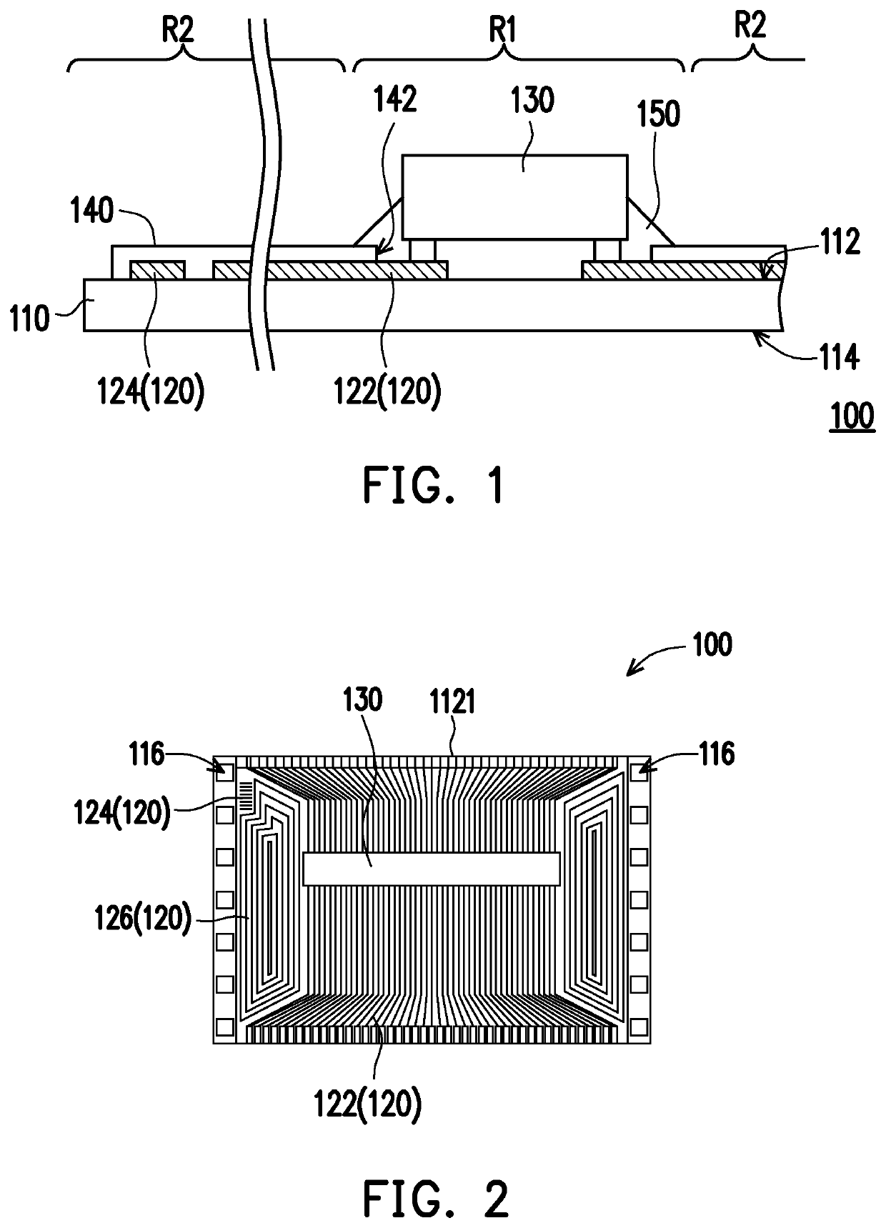
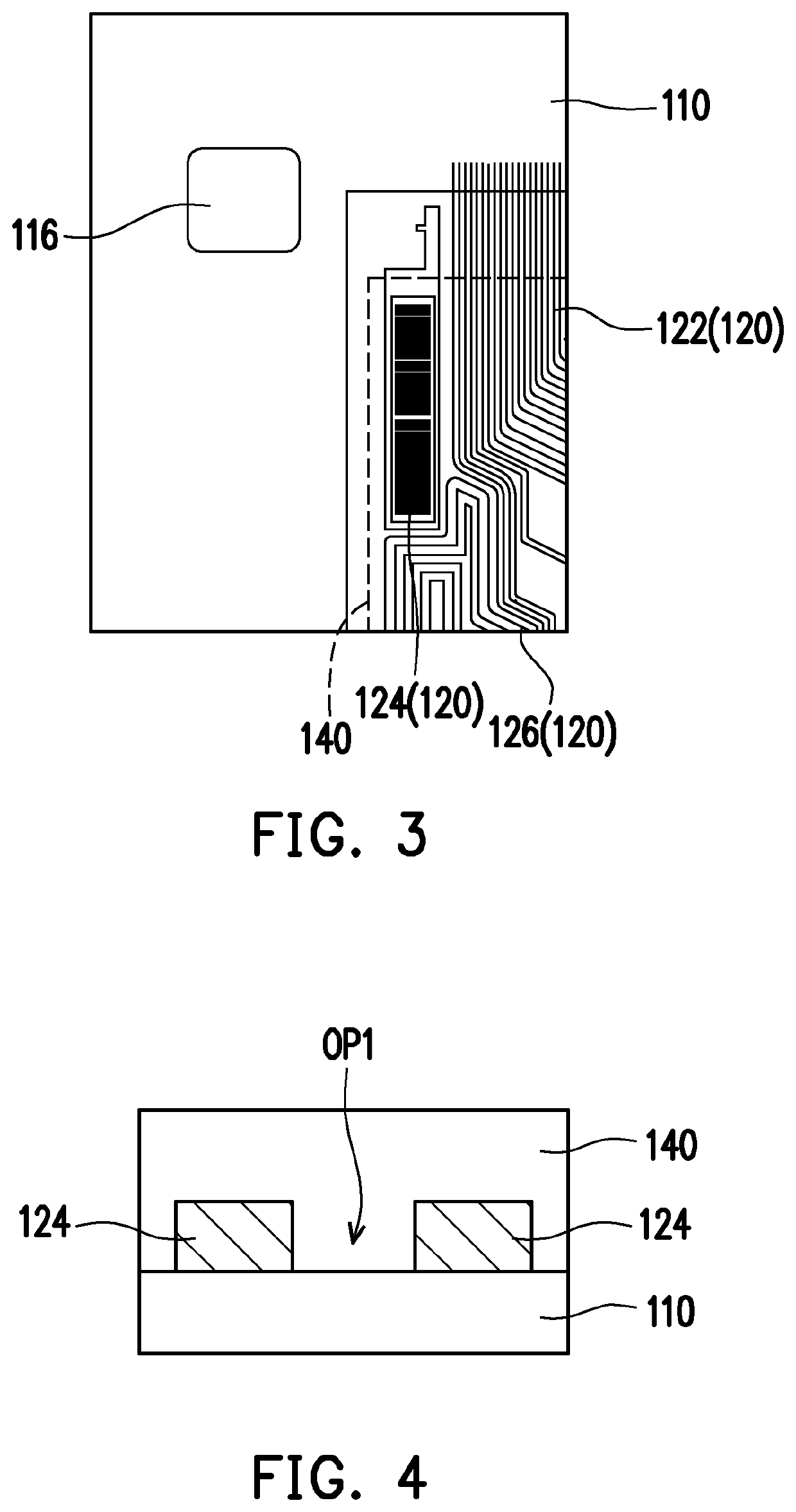
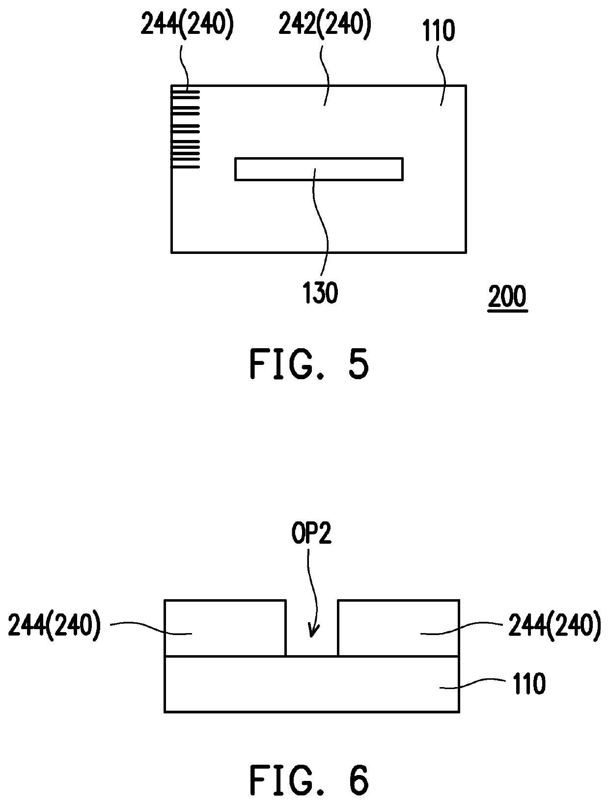
[0033]Reference will now be made in detail to the present preferred embodiments of the disclosure, examples of which are illustrated in the accompanying drawings. Wherever possible, the same reference numbers are used in the drawings and the description to refer to the same or like parts.

[0034]Reference will now be made in detail to the present preferred embodiments of the disclosure, examples of which are illustrated in the accompanying drawings. Wherever possible, the same reference numbers are used in the drawings and the description to refer to the same or like parts. The terms used herein such as “on”, “above”, “below”, “front”, “back”, “left” and “right” are for the purpose of describing directions in the figures only and are not intended to be limiting of the disclosure. Further, in the discussion and claims herein, the term “on” used with respect to two materials, one “on” the other, means at least some contact between the materials, while “over” and “overlie” mean the mater...


PUM

PropertyMeasurementUnit
flexibleaaaaaaaaaa
charge-aaaaaaaaaa
adhesionaaaaaaaaaa

Abstract

A chip on film package structure including a flexible film, a patterned metal layer, a chip, a patterned solder resist layer, and a code-included pattern is provided. The flexible film comprises a chip mounting region and a peripheral region surrounding the chip mounting region. The patterned metal layer disposed on the flexible film. The chip mounted on the chip mounting region and electrically connected to the patterned metal layer. The patterned solder resist layer exposing the chip mounting region and covering a part of the patterned metal layer. The code-included pattern disposed on the peripheral region of the flexible film. The code-included pattern comprises a plurality of machine-readable data. A method for reading a code-included pattern on a package structure is also provided.

Description

CROSS-REFERENCE TO RELATED APPLICATION[0001]This application claims the priority benefits of U.S. provisional application Ser. No. 62 / 787,745, filed on Jan. 2, 2019. The entirety of the above-mentioned patent application is hereby incorporated by reference herein and made a part of specification.BACKGROUNDTechnical Field[0002]The present disclosure generally relates to electronic device and a method. More particularly, the present disclosure relates to a chip on film (COF) package structure and a method for reading a code-included pattern on a package structure.Description of Related Art[0003]Along with the advancement of packaging technology, chip on film (COF) bonding technology has become today's one of the major packaging technologies. Misjudgement or misreading of the product information may reduce the throughput or yield of the production line or the assembly line.SUMMARY[0004]Accordingly, the present disclosure is directed to provide a COF package structure or a method for re...

Claims


Application Information

Patent Timeline
Patent Type & Authority Applications(United States)
IPC IPC(8): H05K1/18H05K1/02H01L23/538
CPCH01L23/5387H05K1/187H05K1/0266H01L23/544G06K7/1413H01L2223/54413H01L23/4985H01L2223/54433H01L2223/54486H05K1/0269H05K2201/09927H05K1/189H05K3/28H01L2224/16225H01L2224/73204H01L2224/32225H01L2924/00
Inventor KUO, TE-HSIEN
Owner NOVATEK MICROELECTRONICS CORP
Why Eureka
Try Eureka