Apparatuses and methods for warpage measurement
- Summary
- Abstract
- Description
- Claims
- Application Information
AI Technical Summary
Benefits of technology
Problems solved by technology
Method used
Image

Examples
Embodiment Construction
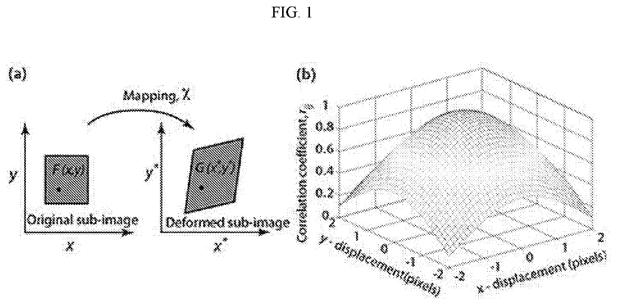
[0012]Global semiconductor packaging and testing market value reached 24.5 billion US dollars in 2014, among which, testing related to warpage is an integral part. The IC chip industry can be divided into chip design, manufacturing and packaging and testing. Warpage measurement analysis figures heavily in each one of these, especially IC packaging and testing such as flip chip BGA board assembly especially with increasing chip size and the use of lead free solders. For example, lead free solders, such as SAC305 are less compliant and have higher reflow temperatures at 260° C. than the older leaded solders, below 230° C. JEDEC specifies that warpage on FCBGA packages must be less than a certain value to assure package reliability. To help this, various material approaches have been developed. The gap between chip and substrate is filled with epoxy underfill to help mitigate the stress induced by the solder bump interconnect. While underfill can protect the solder bumps, it also exace...
PUM
 Abstract
Description
Claims
Application Information
 - R&D Engineer
- R&D Manager
- IP Professional
- Industry Leading Data Capabilities
- Powerful AI technology
- Patent DNA Extraction
Browse by: Latest US Patents, China's latest patents, Technical Efficacy Thesaurus, Application Domain, Technology Topic.
© 2024 PatSnap. All rights reserved.Legal|Privacy policy|Modern Slavery Act Transparency Statement|Sitemap