Laser irradiation method and laser irradiation system

Pending Publication Date: 2020-08-20
GIGAPHOTON +1
View PDF5 Cites 1 Cited by
  • Summary
  • Abstract
  • Description
  • Claims
  • Application Information

AI Technical Summary

Benefits of technology

[0022]a laser irradiation control unit configured to control the stage and the laser apparatus and perform processing of;
[0023]reading, as a first irradiation condition for laser doping, first fluence that is fluence per pulse of the pulse laser beam with which the irradiation region is irradiated and a first irradiation pulse number that is the number of irradiation pulses the irradiation region is irradiated, the number

Problems solved by technology

However, when SiC is doped with impurities by the conventional ion injection method used for

Method used


Image

  • Laser irradiation method and laser irradiation system
  • Laser irradiation method and laser irradiation system
  • Laser irradiation method and laser irradiation system

Examples


first embodiment

3. First Embodiment

[0175]3.1 Configuration

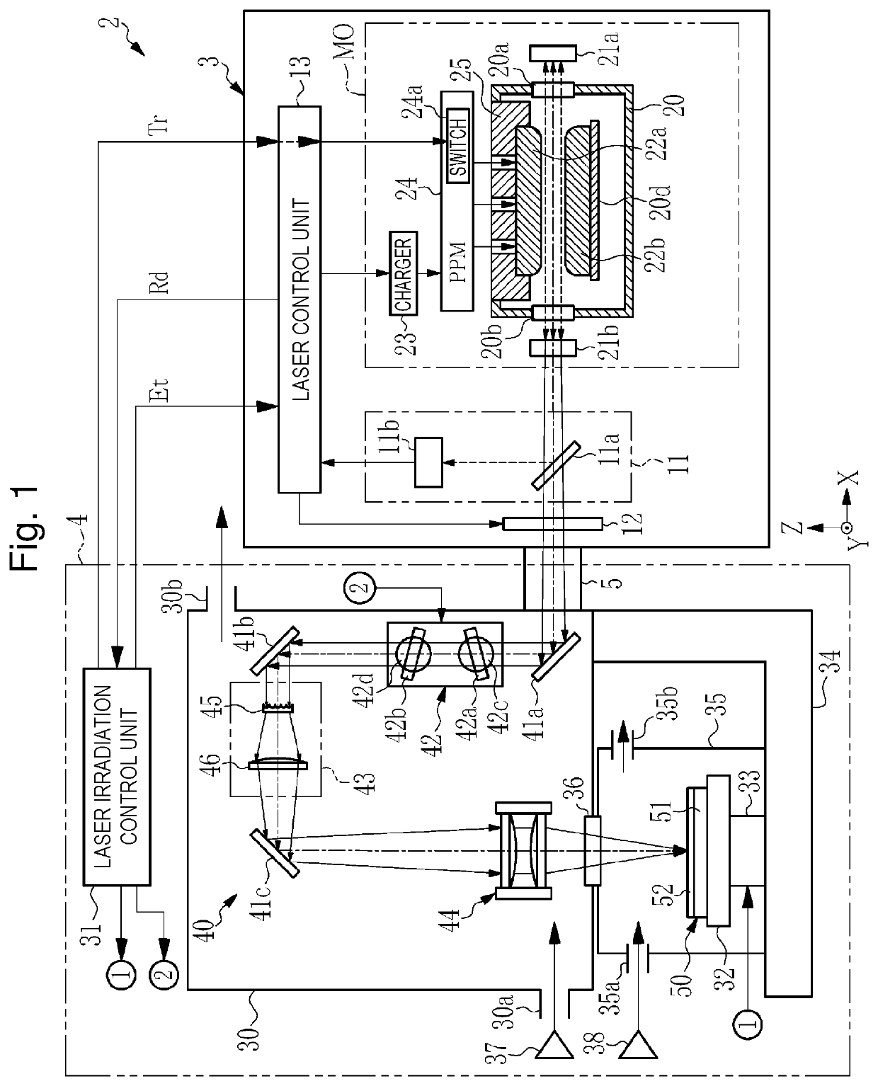
[0176]FIG. 11 schematically illustrates the configuration of a laser irradiation system 2a according to a first embodiment of the present disclosure. The laser irradiation system 2a according to the first embodiment includes a laser apparatus 3a in place of the laser apparatus 3 included in the laser irradiation system 2 according to the comparative example and includes a laser irradiation device 4a in place of the laser irradiation device 4. Hereinafter, a component substantially same as that of the laser irradiation system 2 according to the comparative example is denoted by the same reference sign, and description thereof is omitted as appropriate.

[0177]The laser apparatus 3a includes an optical pulse stretcher (OPS) 10 disposed on the optical path of the pulse laser beam between the master oscillator MO and the monitor module 11. The OPS 10 includes a beam splitter 10y and concave mirrors 10a to 10d. The OPS 10 is disposed so that the be...

second embodiment

4. Second Embodiment

[0232]The following describes a second embodiment. The second embodiment relates to a laser irradiation system configured to dope a semiconductor substrate with impurities by irradiating an irradiation object in which an impurity source film is formed on the semiconductor substrate with a pulse laser beam and to perform post-annealing processing for activating the impurities.

[0233]4.1 Configuration

[0234]The configuration of the laser irradiation system according to the second embodiment is same as that of the laser irradiation system 2a according to the first embodiment. In the present embodiment, the laser irradiation control unit 31 performs post annealing control in addition to laser doping control.

[0235]In the present embodiment, the memory unit of the laser irradiation control unit 31 stores a first irradiation condition of a laser-doping beam and a second irradiation condition of a post-annealing beam. The first irradiation condition includes fluence Fd and...

first modification

5. First Modification

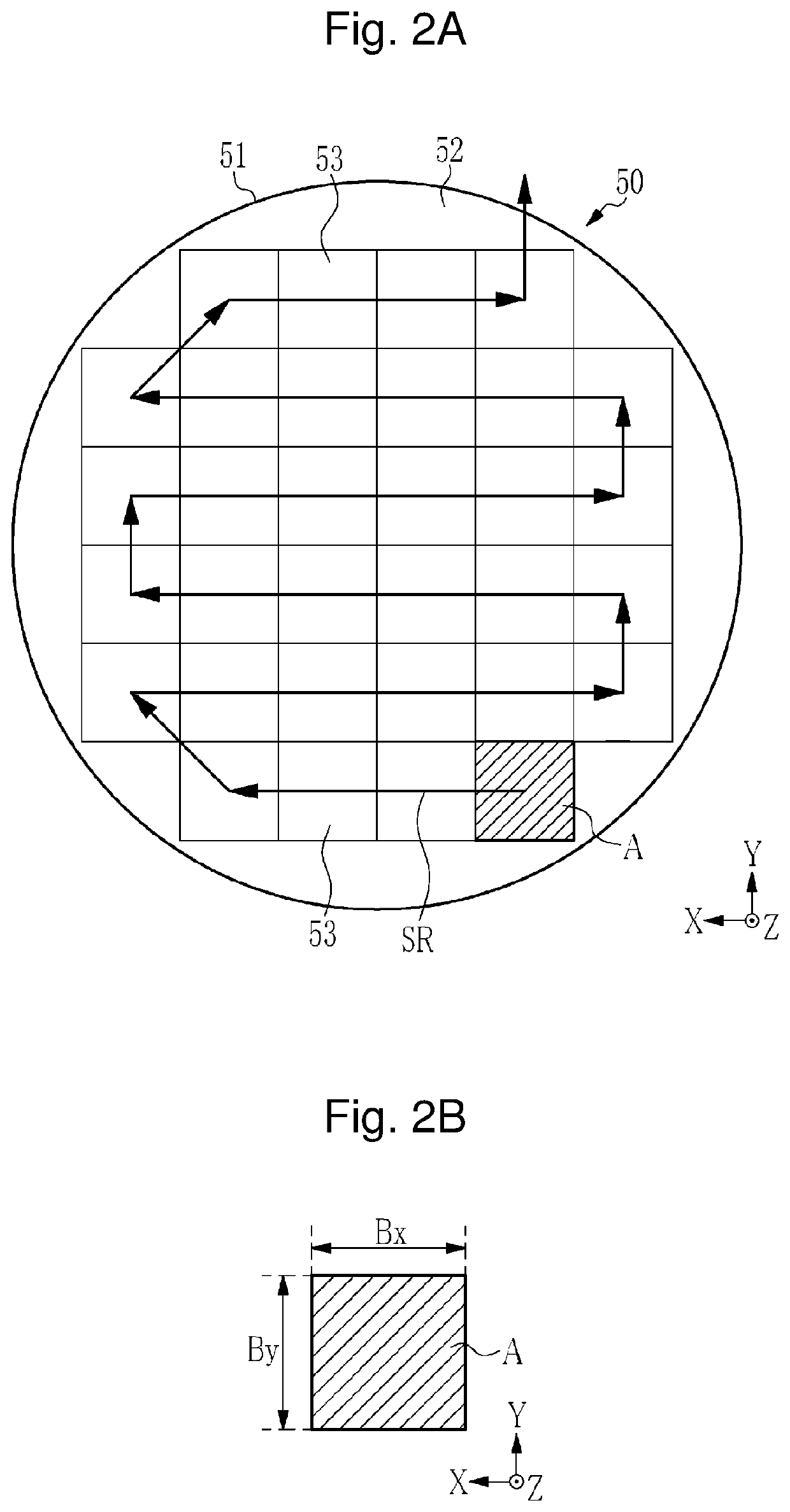
[0289]The following describes a first modification. In the second embodiment, as described with reference to FIG. 19, the post-annealing scanning irradiation is performed after the laser-doping scanning irradiation is performed for each irradiation region A on the irradiation object 50. Instead, the laser-doping scanning irradiation and the post-annealing scanning irradiation may be alternately performed. Specifically, the scanning direction is same between laser doping and post annealing in the second embodiment, but is opposite between laser doping and post annealing in the present modification. The following describes a modification related to the scanning irradiation control in the second embodiment.

[0290]5.1 Scanning Irradiation Control

[0291]FIG. 26 illustrates a first scanning path Sd′ at laser doping and a second scanning path Sp′ at post annealing in the present modification. The first scanning path Sd′ extends in the positive X axial direction. The seco...


PUM

PropertyMeasurementUnit
Thicknessaaaaaaaaaa
Thicknessaaaaaaaaaa
Thicknessaaaaaaaaaa

Abstract

A laser irradiation method of irradiating, with a pulse laser beam, an irradiation object in which an impurity source film is formed on a semiconductor substrate includes: reading fluence per pulse of the pulse laser beam with which a rectangular irradiation region set on the irradiation object is irradiated and the number of irradiation pulses the irradiation region is irradiated, the fluence being equal to or larger than a threshold at or beyond which ablation potentially occurs to the impurity source film when the irradiation object is irradiated with pulses of the pulse laser beam in the irradiation pulse number and smaller than a threshold at or beyond which damage potentially occurs to the surface of the semiconductor substrate; calculating a scanning speed Vdx; and moving the irradiation object at the scanning speed Vdx relative to the irradiation region while irradiating the irradiation region with the pulse laser beam at the repetition frequency f.

Description

CROSS-REFERENCE TO RELATED APPLICATIONS[0001]The present application is a continuation application of International Application No. PCT / JP2017 / 045969, filed on Dec. 21, 2017, the entire contents of which are hereby incorporated by reference.BACKGROUND1. Technical Field[0002]The present disclosure relates to a laser irradiation method and a laser irradiation system.2. Related Art[0003]Semiconductors are materials included in an active element such as an integrated circuit, a power device, a light-emitting diode (LED), a liquid crystal display, or an organic electro luminescence (EL) display, and are absolutely essential in electronic device manufacturing. To manufacture such an active element, a semiconductor substrate needs to be doped with impurities as dopants and then the impurities needs to be activated to control the electric property of the semiconductor substrate to the n-type or the p-type.[0004]Typically, doping of a semiconductor substrate with impurities and activation of...

Claims


Application Information

Patent Timeline
IPC IPC(8): H01L21/78G02F1/01G02B27/09H01S3/11H01S3/225H01S3/23H01L21/223H01L21/268H01L21/67
CPCG02F2203/48H01L21/67115H01S3/225H01S3/11H01L21/223H01L21/78H01S3/2308H01L21/67092G02F1/0121G02B27/0955H01L21/268B23K26/032B23K26/0861B23K26/0732B23K26/352B23K26/127B23K26/123B23K26/0622B23K26/18B23K26/354H01L21/0455H01L29/1608H01S3/0057H01S3/104H01S3/0078H01S3/0071H01S3/005H01S3/0971H01S3/09702
Inventor IKENOUE, HIROSHIWAKABAYASHI, OSAMUOIZUMI, HIROAKISUWA, AKIRA
Owner GIGAPHOTON
Why Eureka
Try Eureka