Resistive random access memory and manufacturing method thereof

Active Publication Date: 2020-08-20
POWERCHIP SEMICON MFG CORP
View PDF2 Cites 1 Cited by
  • Summary
  • Abstract
  • Description
  • Claims
  • Application Information

AI Technical Summary

Benefits of technology

The patent describes a new design for a type of memory called resistive random access memory. This design helps to make the memory more efficient and easy to integrate into other devices. The new design involves using a specific way to access and change the resistance of the memory cells, which allows for a reduction in the amount of space needed for the memory. Overall, this new design improves the performance of resistive random access memory by making it easier to integrate and more efficient in its operation.

Problems solved by technology

Therefore, the volume of resistive random access memory cannot be further reduced due to the device design, resulting in limitation to the integration of resistive random access memory.

Method used


Image

  • Resistive random access memory and manufacturing method thereof
  • Resistive random access memory and manufacturing method thereof
  • Resistive random access memory and manufacturing method thereof

Examples


first embodiment

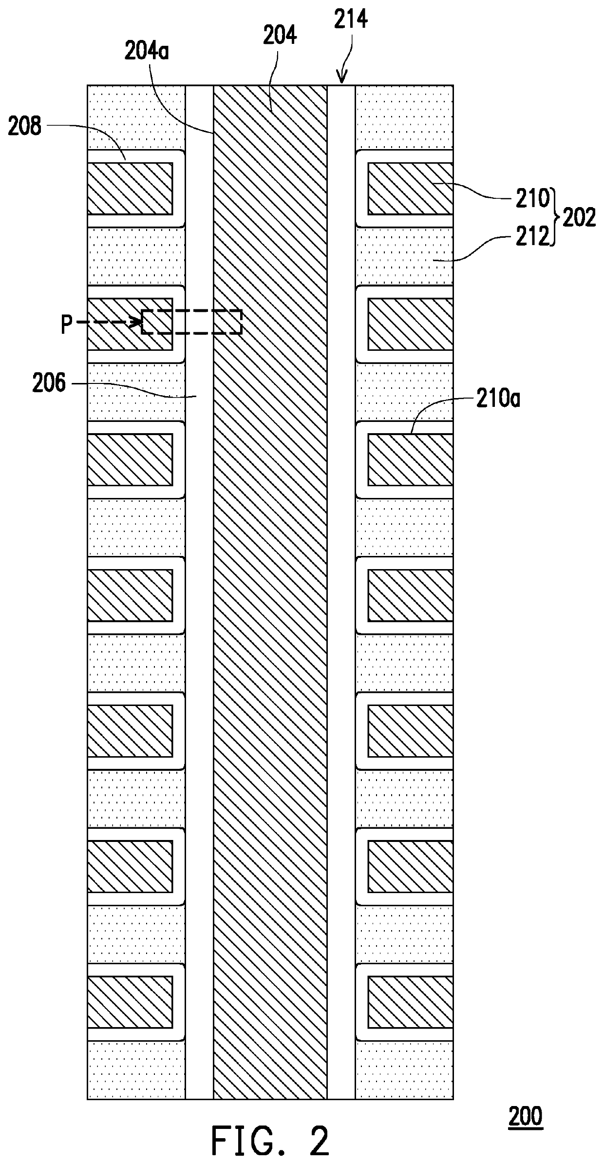
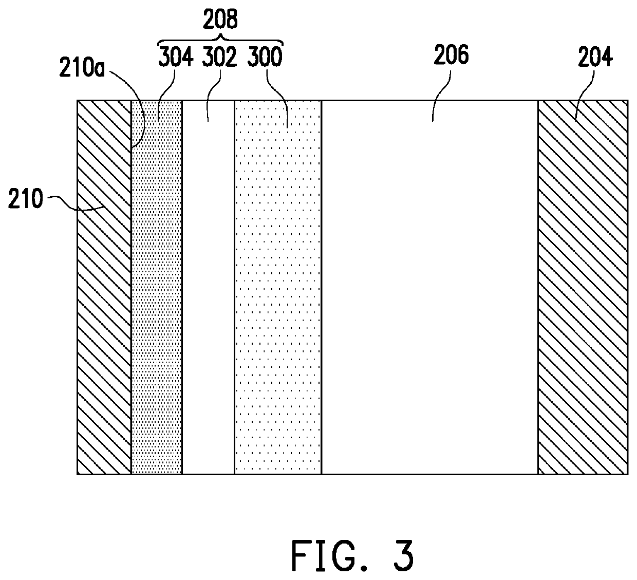
[0033]FIG. 2 is a cross-sectional schematic view of a resistive random access memory according to the disclosure. FIG. 3 is an enlarged schematic view of a portion P of FIG. 2.

[0034]Referring to FIG. 2, a resistive random access memory 200 of the first embodiment includes a stacked structure 202, at least one vertical electrode 204, a selector element 206, and a plurality of resistance changeable structures 208. It shall be stated that although FIG. 2 only illustrates one vertical electrode 204, the number of vertical electrodes 204 may be adjusted according to process design requirements and the disclosure is not limited thereto.

[0035]In the embodiment, the stacked structure 202 is formed by a plurality of horizontal electrodes 210 and a plurality of first dielectric layers 212 stacked alternately. It shall be noted that the number of the horizontal electrodes 210 and the first dielectric layers 212 illustrated in FIG. 2 is respectively 7 layers and 8 layers, and the horizontal ele...

second embodiment

[0039]FIG. 4 is a cross-sectional schematic view of a resistive random access memory according to the disclosure. FIG. 5A, FIG. 5B, and FIG. 5C are respectively a portion P1, a portion P2, and a portion P3 of FIG. 4.

[0040]Referring to FIG. 4, the difference between a resistive random access memory 400 and the resistive random access memory 200 lies in the difference between the structure of a selector element 406 and the structure of the selector element 206. For example, the selector element 406 is, for example, a MOS device including a gate layer 410, a gate insulating layer 412, and a channel layer 414. The gate layer 410 is in contact with the vertical electrode 204, the channel layer 414 is in contact with the oxide layer 300 (as shown in FIG. 5B), and the gate insulating layer 412 is disposed between the channel layer 414 and the gate layer 410. Since the MOS device of the second embodiment is present in the channel hole 214, as compared to FIG. 1 which sets the MOS device in ...


PUM


Abstract

A resistive random access memory including a stacked structure, at least one vertical electrode, a selector element, and a plurality of resistance changeable structures is provided. The stacked structure is formed by a plurality of horizontal electrodes and a plurality of first dielectric layers stacked alternately, wherein the stacked structure has at least one channel hole extending through the horizontal electrodes and the first dielectric layers. The vertical electrode is formed in the at least one channel hole. The selector element is formed in the channel hole between the vertical electrode and the stacked structure. The resistance changeable structures are disposed on the surface of each of the horizontal electrodes and are in contact with the selector element in the channel hole.

Description

CROSS-REFERENCE TO RELATED APPLICATION[0001]This application claims the priority benefit of Taiwan application serial no. 108105177, filed on Feb. 15, 2019. The entirety of the above-mentioned patent application is hereby incorporated by reference herein and made a part of specification.BACKGROUNDTechnical Field[0002]The disclosure relates to a random access memory and a manufacturing method thereof, and more particularly to a resistive random access memory and a manufacturing method thereof.Description of Related Art[0003]Resistive random access memory (RRAM) has become one of the most promising non-volatile memory technologies currently due to its superior scalability, ease of operation, low power consumption, and relatively simple process.[0004]As shown in FIG. 1, the constitution of a conventional resistive random access memory 100 mostly includes a vertical electrode 102, a resistance changeable layer 104, a horizontal electrode 106, a bit line 108, a word line 110 composed of ...

Claims


Application Information

Patent Timeline
IPC IPC(8): H01L27/24H01L45/00
CPCH01L45/1253H01L27/2436H01L45/145H10B43/30H10B63/24H10B63/34H10B63/845H10B63/20H10N70/823H10N70/20H10N70/883H10B63/30H10N70/841
Inventor WANG, ZIH-SONG
Owner POWERCHIP SEMICON MFG CORP
Why Eureka
Try Eureka