LED filament and lamp, and manufacturing process of LED filament

a manufacturing process and technology of led filament, applied in the direction of printed circuit non-printed electric components association, lighting and heating apparatus, lighting support devices, etc., can solve the problems of increased material cost, increased manufacturing procedures, and easy defects during manufacturing and multiple welding processes, so as to achieve low manufacturing cost, high defect rate in manufacturing, and low manufacturing efficiency

Active Publication Date: 2020-10-15
HANGZHOU BINARY OPTOELECTRONICS & TECH CO LTD
View PDF0 Cites 1 Cited by
  • Summary
  • Abstract
  • Description
  • Claims
  • Application Information

AI Technical Summary

Benefits of technology

[0008]In view of the deficiencies in the prior art, the present disclosure provides an LED filament and lamp, and a manufacturing process of an LED filament, so as to solve the problem in the prior art that the LED filaments have high defect rate in manufacturing, high cost and low manufacturing efficiency, and are easy to break.
[0042]For the present LED filament, the LED chips are connected on a PCB substrate as a lampwick, and different from the conventional brittle lampwick substrate such as ceramic and glass, the PCB substrate has relatively good toughness and has no stress concentration, and the lampwick of the LED filament cannot be easily destroyed under the action of vibration and external forces. While electrical connection is formed between the LED chips and the connecting circuit, heat conduction is also formed between the LED chips and the PCB substrate. Thus, the LED filament has superior heat dissipation effect. The PCB substrate is suitable for various circuit arrangements, and different connecting circuits can be drawn according to requirements. The LED chips, the LED chips and the positive pins, and the LED chips and the negative pins do not need to be powered on by wires, which omits the use of metal wires, and leads to a simpler connecting process of the LED chips, and lower manufacturing cost. Moreover, the connecting circuit etched on the PCB substrate has good mechanical strength and relatively good stability, thereby making the quality of the LED filament more stable and reducing the defects in the LED filament.
[0043]The lamp comprises the LED filament, which has better durability, and the assembly of the LED filament of the lamp can be simplified by reasonably arranging the power connection pins on the LED filament.
[0044]For the manufacturing process of an LED filament, a PCB substrate is used as a base material, a connecting circuit is fabricated on the PCB substrate, the connecting circuit is directly used for connecting an LED chip, and there is no necessity to perform welding by using wires, which reduces the manufacturing cost and improves the manufacturing efficiency and the manufacturing yield rate; and the LED filament manufactured by this method has a more stable electrical connection structure, and is suitable for mass production.

Problems solved by technology

1. Defects will easily occur during the manufacturing and multiple welding processes of the LED filaments.
2. Welding metal wires increases the material cost, leads to more manufacturing procedures and low manufacturing efficiency, and also results in unstable electrical connection and poor electrical conductivity.
3. The substrates such as ceramic, glass and sapphire are brittle, are easy to break, and have high transportation and storage costs, but low service life.

Method used


Image

  • LED filament and lamp, and manufacturing process of LED filament
  • LED filament and lamp, and manufacturing process of LED filament
  • LED filament and lamp, and manufacturing process of LED filament

Examples


embodiment 1

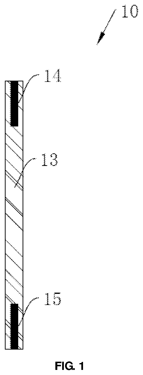
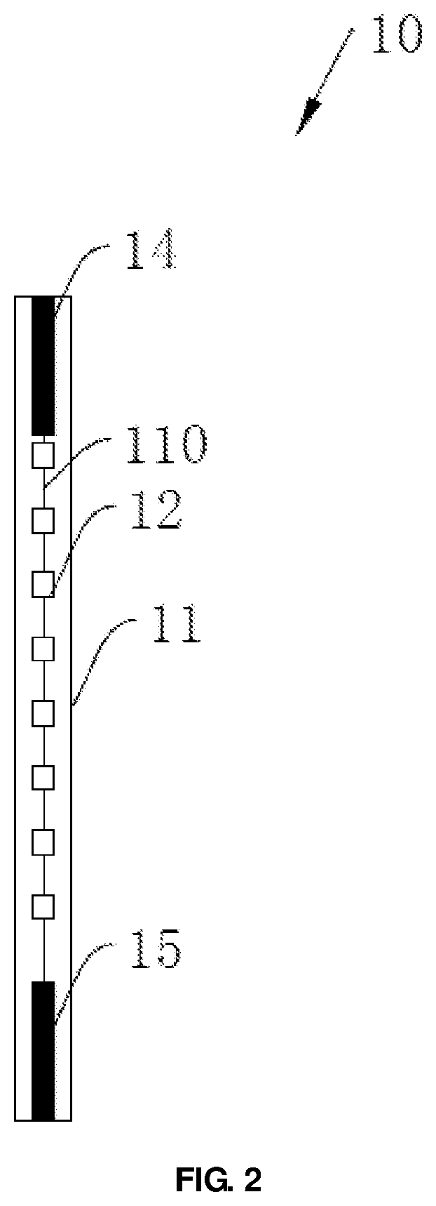
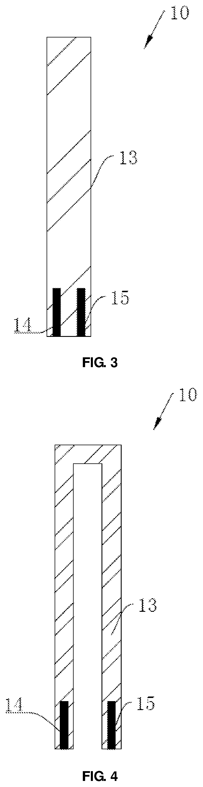
[0082]Optionally, referring to FIG. 4 and FIG. 5 together, this embodiment is distinguished in that the shape of the LED filament 10 is non-strip-shaped or non-column-shaped, that is, the PCB substrate 11 is not strip-shaped. The PCB substrate 11 comprises electrode arms 111 and a connecting arm 112, one ends of the two electrode arms 111 are connected by the connecting arm 112, and the other ends of the two electrode arms 111 are provided with a positive pin 14 and a negative pin 15, respectively. The PCB substrate 11 is a specially-shaped substrate, and the LED filament 10 is a specially-shaped filament.

[0083]Further, the PCB substrate 11 has a shape of “”, wherein the electrode arms 111 and the connecting arm 112 are in strip-shape, and the positive pin 14 and the negative pin 15 are provided on the two sides of the opening of the PCB substrate 11, that is, they are respectively provided at the hanging ends of the electrode arms 111. The connecting circuit 110 extends from the po...

embodiment 2

[0092]As shown in FIG. 9, in another embodiment, the lamp 1 comprises a lamp holder 20 and the LED filament 10 in embodiment 2. The lamp holder 20 is provided with four insertion holes 201 arranged in a cross shape, in other words, the connecting lines of each pair of opposite insertion holes 201 are arranged in a cross.

[0093]In the insertion hole 201 are correspondingly provided positive and negative electrical contacts or positive and negative electrical elastic pieces. It is feasible to insert one “”-shaped LED filament 10 into two opposite insertion holes 201, or insert two LED filaments 10 into four insertion holes 201 to form a three-dimensional filament.

[0094]Optionally, as shown in FIGS. 11 and 12, the present disclosure provides a structural schematic view of an LED lamp comprising the LED filament provided by the present disclosure. The LED lamp provided in the present disclosure includes, but is not limited to, the following lamp forms: bulb lamps, ceiling lamps, ceiling ...


PUM

PropertyMeasurementUnit
stress concentrationaaaaaaaaaa
two-dimensional shapeaaaaaaaaaa
conductiveaaaaaaaaaa

Abstract

An LED filament and lamp, and a manufacturing process of an LED filament the LED filament includes a PCB substrate and multiple LED chips, connecting circuits are provided on the PCB substrate, a positive pin and a negative pin are provided at two ends of the connecting circuit, respectively, and each LED chip is electrically connected to the connecting circuit; and a fluorescent glue layer is provided outside the PCB substrate and the LED chips, and the positive pin and the negative pin are exposed from the fluorescent glue layer. The LED lamp includes the LED filament. The manufacturing process of an LED filament enables manufacturing an LED filament. For the LED filament and lamp, and the manufacturing process of an LED filament, a PCB substrate is used as a base material, connecting circuits are fabricated on the PCB substrate, the connecting circuits are directly used for connecting LED chips.

Description

CROSS-REFERENCE TO RELATED APPLICATIONS[0001]The present disclosure claims the priority of the Chinese Application No. 2018113118531, filed with the Chinese Patent Office on Nov. 6, 2018 and entitled “LED Filament and Lamp, and Manufacturing Process of LED Filament”, which is incorporated herein by reference in its entirety.TECHNICAL FIELD[0002]The present disclosure relates to the field of LED illumination, and particularly to an LED filament and lamp, and a manufacturing process of an LED filament.BACKGROUND ART[0003]For most of the existing conventional LED filaments, ceramic, glass and sapphire are used as a substrate, on which an LED chip is mounted, and then the LED chip is powered on by using a noble metal wire.[0004]The existing LED filaments have the following defects:[0005]1. Defects will easily occur during the manufacturing and multiple welding processes of the LED filaments.[0006]2. Welding metal wires increases the material cost, leads to more manufacturing procedures ...

Claims


Application Information

Patent Timeline
Patent Type & Authority Applications(United States)
IPC IPC(8): F21K9/235F21V9/30F21V19/00F21K9/232F21K9/90H05K1/11H05K1/03H05K1/18H05K1/14
CPCH05K1/14F21K9/232H05K2201/10318H05K1/117H05K2201/0108H05K2201/10106F21K9/235F21V9/30F21Y2115/10H05K1/181F21K9/90F21V19/005F21Y2107/50H05K2201/09027H05K1/0366H05K2201/09163F21V19/001F21V21/02F21V23/06F21K9/20
Inventor ZHANG, GAOLEZHOU, KANG
Owner HANGZHOU BINARY OPTOELECTRONICS & TECH CO LTD
Why Eureka
Try Eureka