Method of forming an electronic structure using reforming gas, system for performing the method, and structure formed using the method

Active Publication Date: 2020-12-17
ASM IP HLDG BV
View PDF0 Cites 127 Cited by
  • Summary
  • Abstract
  • Description
  • Claims
  • Application Information

AI Technical Summary

Benefits of technology

[0007]Various embodiments of the present disclosure relate to methods of forming high-quality films using PE-ALD. While the ways in which various embodiments of the present disclosure address drawbacks of p

Problems solved by technology

However, with miniaturization of devices, it becomes increasingly difficult to conformally deposit material, particularly over high aspect ratio features, such as features having an aspect ratio of three or more.
Unfortunately, material deposited using PE-ALD can exhibi

Method used


Image

  • Method of forming an electronic structure using reforming gas, system for performing the method, and structure formed using the method
  • Method of forming an electronic structure using reforming gas, system for performing the method, and structure formed using the method
  • Method of forming an electronic structure using reforming gas, system for performing the method, and structure formed using the method

Examples


Embodiment Construction

[0021]Although certain embodiments and examples are disclosed below, it will be understood by those in the art that the invention extends beyond the specifically disclosed embodiments and / or uses of the invention and obvious modifications and equivalents thereof. Thus, it is intended that the scope of the invention disclosed should not be limited by the particular disclosed embodiments described below.

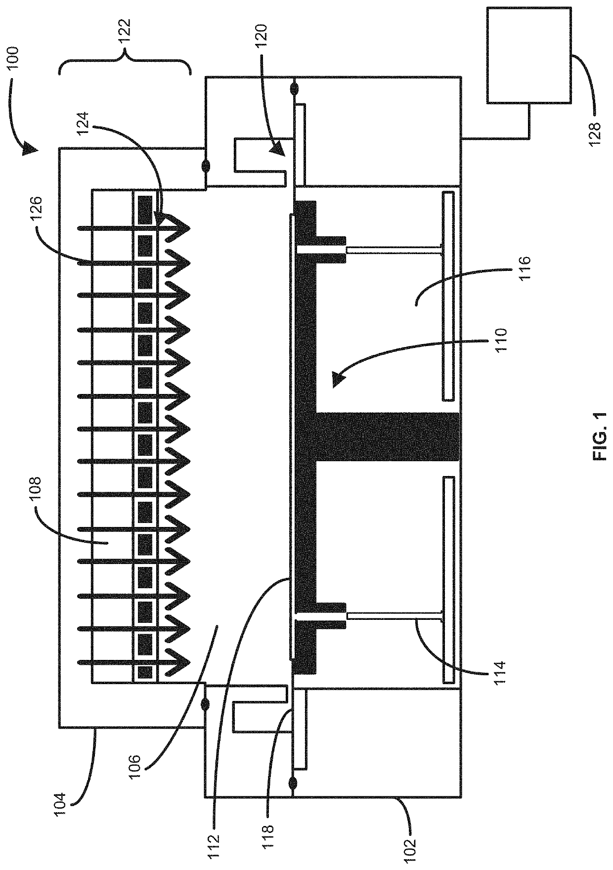
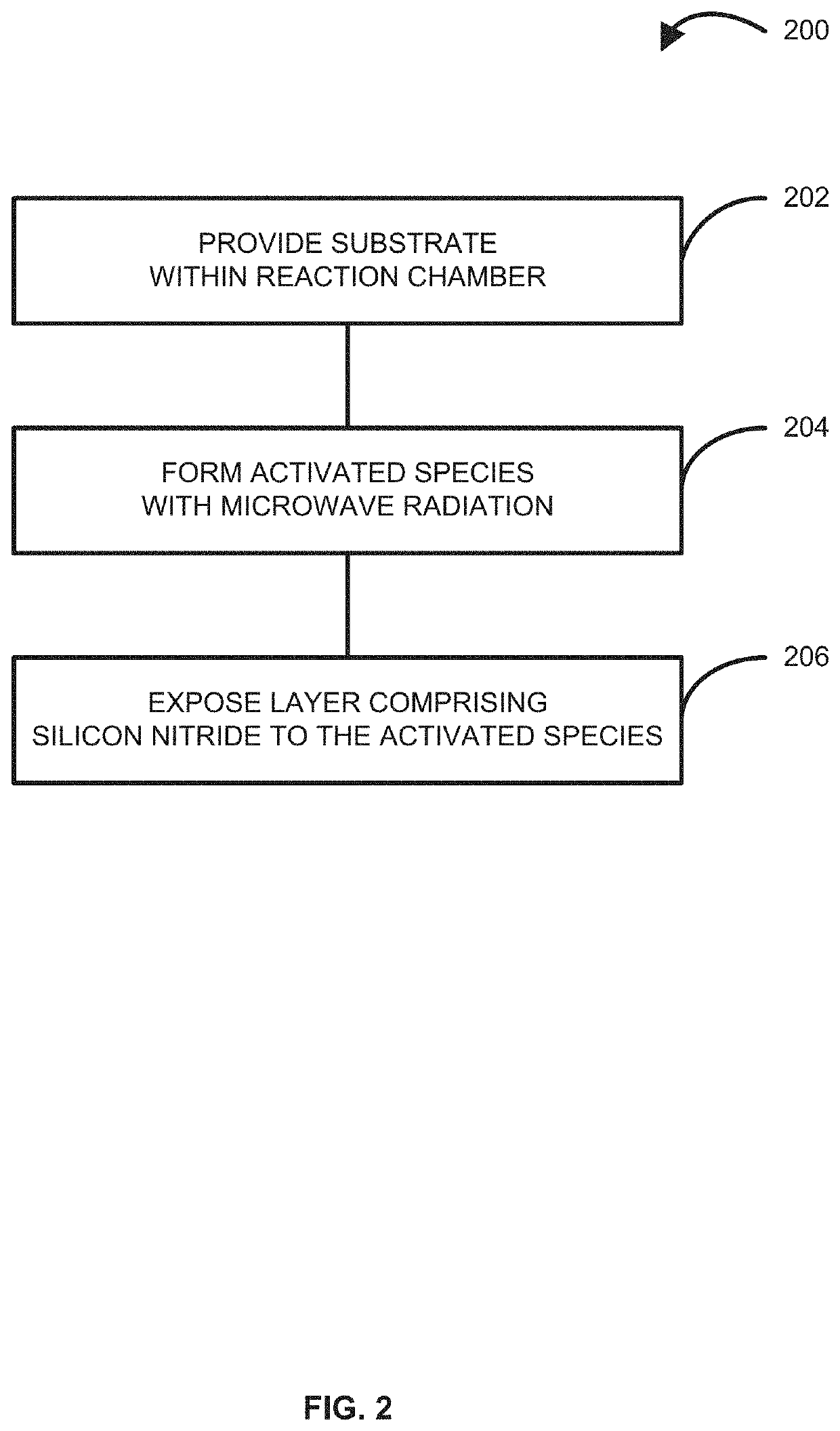
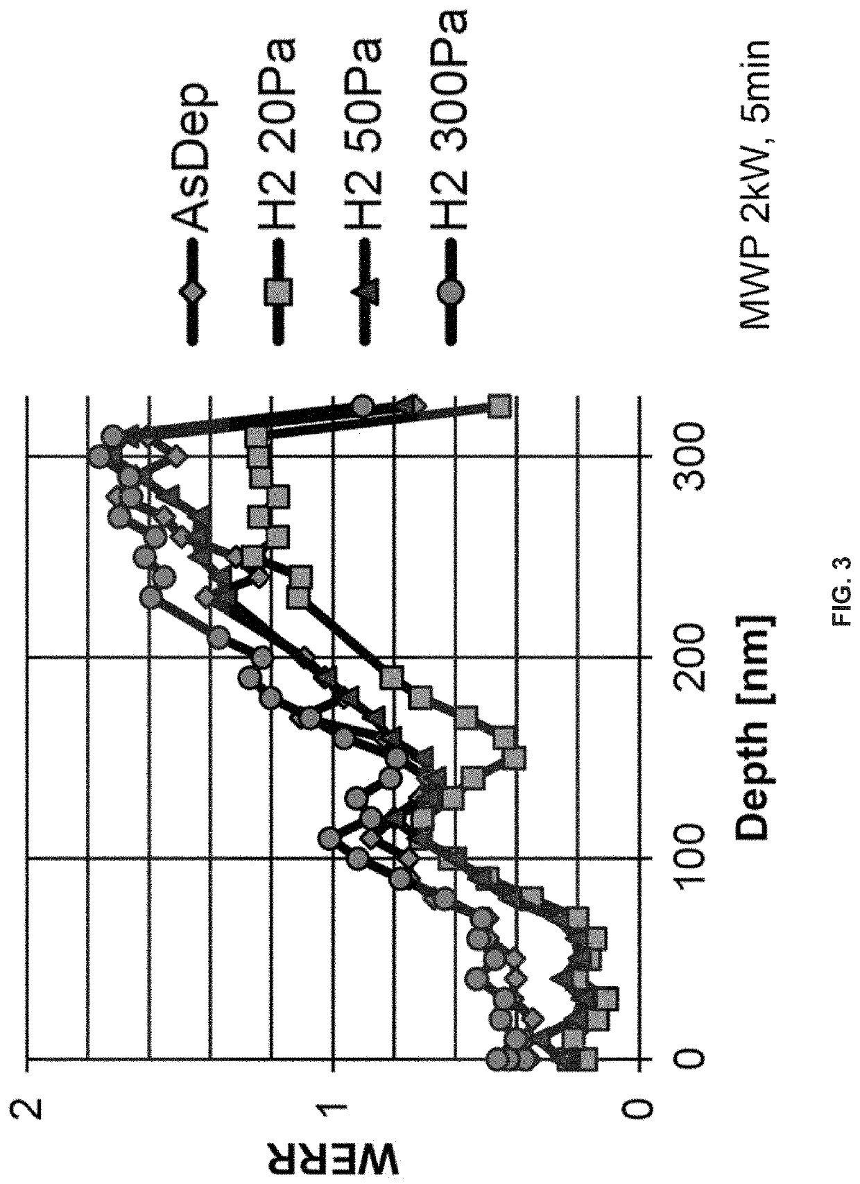
[0022]The present disclosure generally relates to methods of forming electronic device structures, to deposition apparatus for performing the methods, and to structures formed using the method. By way of examples, the systems and methods described herein can be used to form high-quality silicon nitride films. The silicon nitride films can be deposited (e.g., conformally) using PE-ALD onto a surface of a substrate, which can include high-aspect ratio features. The PE-ALD deposited material can then be exposed to activated species formed by irradiating a reforming gas with microwave radi...


PUM

PropertyMeasurementUnit
Temperatureaaaaaaaaaa
Fractionaaaaaaaaaa

Abstract

Methods of and systems for reforming films comprising silicon nitride are disclosed. Exemplary methods include providing a substrate within a reaction chamber, forming activated species by irradiating a reforming gas with microwave radiation, and exposing substrate to the activated species. A pressure within the reaction chamber during the step of forming activated species can be less than 50. Pa.

Description

CROSS-REFERENCE TO RELATED APPLICATIONS[0001]This application claims the benefit of U.S. Provisional Patent Application No. 62 / 860,158 filed on Jun. 11, 2019, the disclosure of which is incorporated herein in its entirety by reference.FIELD OF INVENTION[0002]The present disclosure generally relates to methods of treating material on a surface of a substrate, to structures formed using the method, and to systems for treating the material.BACKGROUND OF THE DISCLOSURE[0003]Conformal film deposition may be desirable for a variety of reasons. For example, during the manufacture of devices, such as semiconductor devices, it is often desirable to conformally deposit material over features formed on the surface of a substrate. Such techniques can be used for shallow trench isolation, inter-metal dielectric layers, passivation layers, and the like. However, with miniaturization of devices, it becomes increasingly difficult to conformally deposit material, particularly over high aspect ratio ...

Claims


Application Information

Patent Timeline
IPC IPC(8): H01L21/02H01L21/285
CPCH01L21/28518H01L21/0217H01L21/0228H01L21/3105H01L21/67011H01L29/66795H01L29/785H10B41/35H10B41/20H10B43/35H10B43/20H01L21/02274H01L21/0234H01L21/68742H01L21/76831H01L21/76826C23C16/511C23C16/452C23C16/45557C23C16/45536C23C16/045C23C16/54H01L21/31111H01J37/32201
Inventor YOSHIMOTO, SHINYAYOSHIKAWA, JUNNOZAWA, TOSHIHISA
Owner ASM IP HLDG BV
Why Eureka
Try Eureka