Thermoelectric conversion device and method for manufacturing the same

a technology of conversion device and thermal conversion device, which is applied in the manufacture/treatment of thermoelectric device, thermoelectric device details, and thermoelectric device junction materials. it can solve the problems of inability to meet the technical requirements of direct silicon containing material-metal interconnection, inability to meet the technical requirements of electrically conductive interconnection, and inability to use materials. to achieve the effect of overcompensation or reducing the number o

Active Publication Date: 2020-12-31
RGS DEVMENT
View PDF0 Cites 0 Cited by
  • Summary
  • Abstract
  • Description
  • Claims
  • Application Information

AI Technical Summary

Benefits of technology

[0017]It is an object of the present invention to provide a thermoelectric conversion device based on silicon, silicon composites, silicon alloys or metal-silicide based materials and a method for manufacturing a thermoelectric conversion device that overcomes or mitigates the above detrimental effects.

Problems solved by technology

However due to the material properties of bismuth telluride materials, such devices are typically limited to a maximum operating temperature of 250° C. In the so called high-temperature range with hot side device operating temperatures of more than 500° C., these materials are no longer useful.
However due to the high operating temperatures and the long intended operational lifetime of a thermoelectric generator the technical requirements for these electrically conductive interconnections are extremely demanding.
The accepted state-of-the-art is that a direct silicon containing material-metal interconnection cannot meet the technical requirements above.
The reasons for that are that metals from the metal interconnection layer will diffuse into the thermoelectric (silicide) material and degrade the electrical properties while silicon from the thermoelectric material will react with the metal interconnection forming often very brittle metal silicides at the interface.
As these diffusion processes will continue during device operation, such an interconnection is not stable under operation.
Additionally silicon, silicon composites, silicon alloys or metal-silicide based material-metal interconnects often show differences in thermal expansion coefficient that lead to thermal stress in the interconnection and to crack formation or breakage of the interconnection.
However, in our test results the proposed structure including a manganese silicide—Ni interface was not stable under long term operation in a high temperature environment.
Such a system is expected to have a limited lifetime under high temperature operation.
Such a structure provides low electrical resistance contacts to the thermoelectric material itself, however it is not useful for thermoelectric module manufacturing, as transition metal silicides are mechanically not sufficiently stable and in combination with a metal such e.g. Ni will not prevent silicon diffusion into the metal and finally conversion of the metal layer into metal silicide.
Such a method will not produce a stable silver metal interconnection and is subject to further sintering of the Ag particles during thermoelectric operations and thus very likely unstable.
In general the prior art disclosures to produce low resistivity electrical contacts to silicides lack long term stability due to the diffusion of either metal components of the contacts into the thermoelectric silicide material or silicon from the thermoelectric material into the metallization layer where undesired or detrimental silicides are formed that often form a mechanically brittle material.
In addition differences in thermal expansion coefficient lead to high thermal stress in the interconnection and can result in crack forming and finally breakage of the contacts.
At lower temperatures such a p-n junction is not sufficiently conductive, therefore p-n junction based thermoelectric devices are limited in performance at low and medium temperatures (depending upon the bandgap of the materials, ohmic conduction of a p-n junction might require temperatures of at least 500° C. or above).
In summary, the state of the art in thermoelectric devices based upon silicon containing materials such as silicon, silicon composites, silicon alloys or metal-silicides based materials is that high conductivity Schottky type contacts between the semiconductor and an interconnection metal are not sufficiently stable due to metal silicide formation at the interface and metal interdiffusion into the semiconductor materials.
The direct interconnection between two silicon, silicon composites, silicon alloys or metals silicides thermoelectric elements in the form of a p-n junction can result in a stable interconnection, however at a reduced device performance due to the higher resistivity of a p-n junction.

Method used


Image

  • Thermoelectric conversion device and method for manufacturing the same
  • Thermoelectric conversion device and method for manufacturing the same
  • Thermoelectric conversion device and method for manufacturing the same

Examples


Embodiment Construction

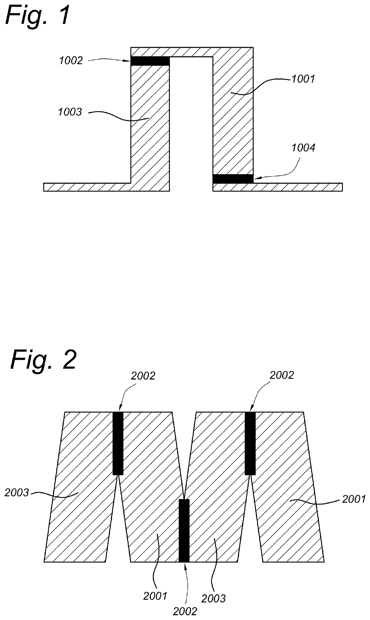
[0040]FIG. 1 shows a cross-sectional view of a thermoelectric conversion device according to an embodiment of the present invention.

[0041]According to an embodiment, a thermoelectric conversion device comprises a plurality of thermoelectric elements 1001 and 1003, also denoted as “active elements”, from a silicon, silicon composites, silicon alloys or metal-silicide based material. Such thermoelectric elements may have a shape of a bar.

[0042]Each thermoelectric element 1001; 1003 comprises a contact interface to an interconnection zone 1002 and a second interconnection zone 1004; For example, these contact and counter interfaces are formed at the respective ends of the bar shape. During use of the thermoelectric element one contact interface (e.g., the first contact interface) is kept at a relatively high temperature, i.e., a hot side positioned in a zone with relatively high temperature and the other, first counter interface as cold side is kept at relatively low temperature, posit...


PUM

PropertyMeasurementUnit
thicknessaaaaaaaaaa
thicknessaaaaaaaaaa
operating temperaturesaaaaaaaaaa

Abstract

A thermoelectric device includes active elements containing thermoelectric materials of silicon, an alloy of silicon, a metal-silicide or silicon composite and an interconnection zone consisting of a metal interconnect and a re-crystallized phase consisting of material from the active thermoelectric elements. The metal interconnect is from a metal that does not form metal silicides in a solid state, has a certain solubility for components of the thermoelectric elements in the liquid phase and a low solubility of these components in the solid phase. The active thermoelectric elements are shaped with a first and a second contact interface. The interconnection between the different thermoelectric elements consists of at least two phases of material, one of which is mainly the metallic interconnection material, the other is formed by the re-crystallized components of the thermoelectric materials.

Description

FIELD OF THE INVENTION[0001]The present invention relates to a thermoelectric conversion device made from a silicon containing material. Additionally, the invention relates to a method for manufacturing such a thermoelectric conversion device.BACKGROUND[0002]Thermoelectric elements based upon bismuth telluride containing materials are well known and largely applied in different applications. However due to the material properties of bismuth telluride materials, such devices are typically limited to a maximum operating temperature of 250° C. In the so called high-temperature range with hot side device operating temperatures of more than 500° C., these materials are no longer useful.[0003]On the other side, silicon, silicon composites, silicon alloys and metal-silicide based thermoelectric conversion devices offer the promise to become low cost, environmentally benign thermoelectric devices that are very well suited for high temperature operation with device hot side temperatures abov...

Claims


Application Information

Patent Timeline
Patent Type & Authority Applications(United States)
IPC IPC(8): H01L35/08H01L35/22H01L35/34
CPCH01L35/34H01L35/08H01L35/22H10N10/81H10N10/855H10N10/01H10N10/817
Inventor SCHÖNECKER, AXEL GEORGPICHON, PIERRE-YVESVAN SCHAIK, WILHELMUS GERARDUS ADRIANUS
Owner RGS DEVMENT
Why Eureka
Try Eureka