

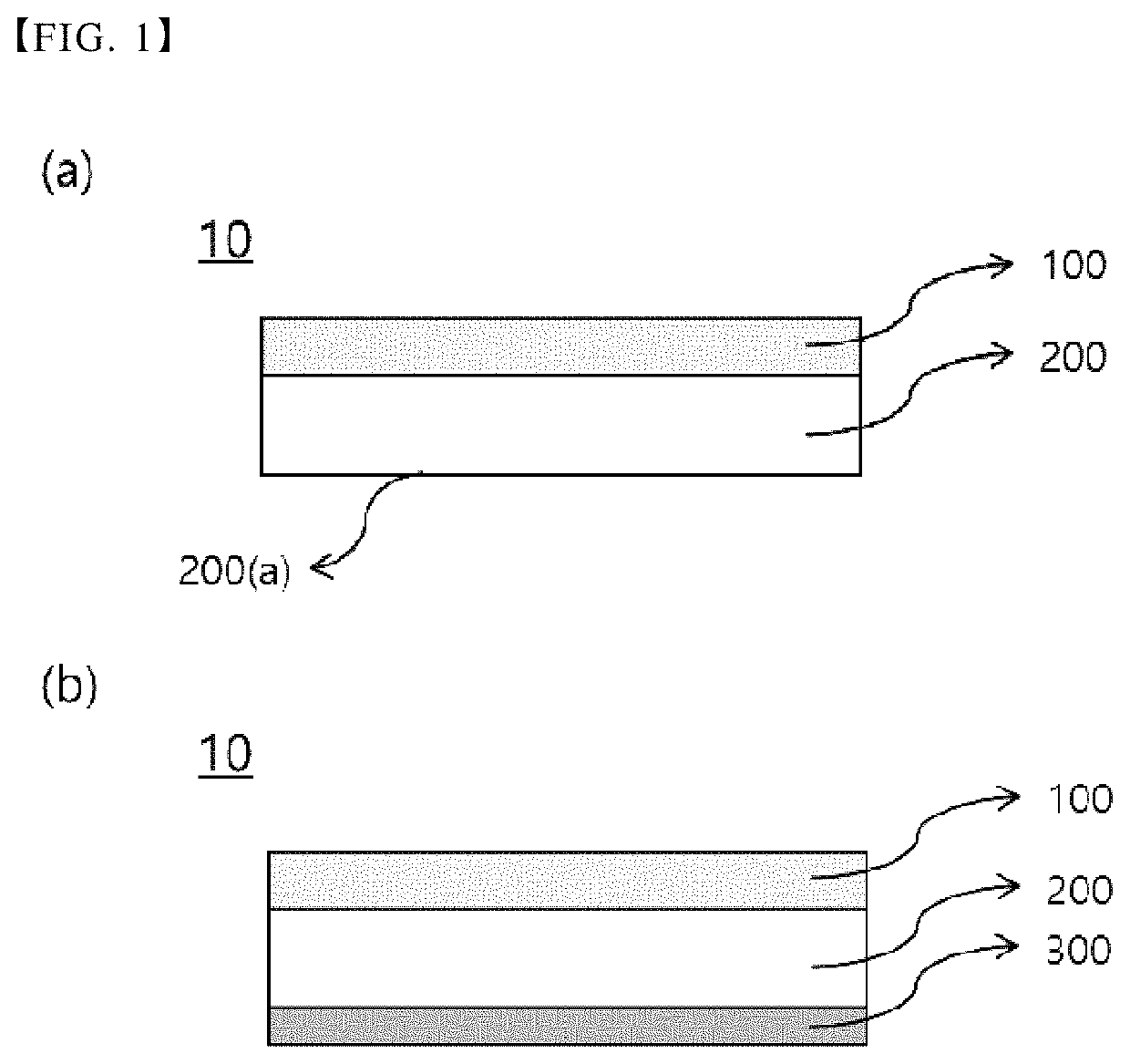
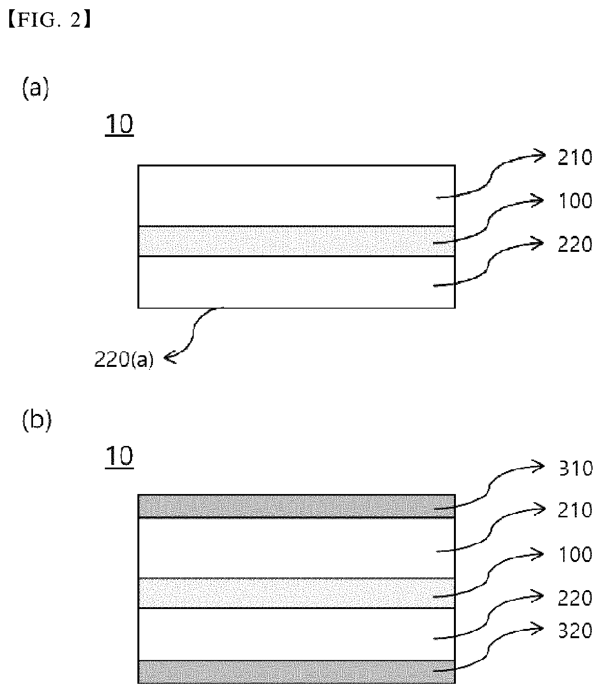
Adhesive sheet for temporary attachment and method for producing semiconductor device using the same
- Summary
- Abstract
- Description
- Claims
- Application Information
AI Technical Summary
Benefits of technology
Problems solved by technology
Method used
Image

Examples
preparation examples
sition for Forming Adhesive Layer
preparation example 1
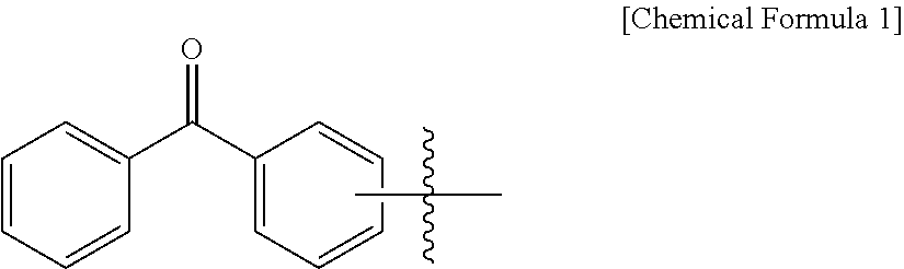
[0128]A monomer mixture consisting of 75 g of 2-ethylhexyl acrylate (2-EHA), 5 g of 4-benzoylphenylmethacrylate, and 20 g of hydroxyethyl acrylate (HEA) was put into a reactor equipped with a cooling system so as to achieve reflux of a nitrogen gas and ease of temperature control.
[0129]Subsequently, 400 pm of n-DDM (n-dodecyl mercaptan) as a chain transfer agent (CTA) and 100 g of ethyl acetate (EAc) as a solvent based on 100 g of the monomer mixture were added thereto, and sufficiently mixed with each other at 30° C. for 30 minutes or more while injecting nitrogen in order to remove oxygen in the reactor.
[0130]Then, the temperature was increased to and maintained at 62° C., and V-60 (azobisisobutyronitrile) at 300 ppm as a reaction initiator was added thereto to thereby initiate the reaction, followed by polymerization for 6 hours to prepare a primary reaction material.
[0131]24 g of 2-methacyloxyethyl isocyanate (MOI) (90 mol % based on HEA in the primary reaction material) and 0.2...
preparation example 2
[0133]A monomer mixture consisting of 20 g of ethyl acrylate, 63 g of 2-ethylhexyl acrylate (2-EHA), 2 g of 4-benzoylphenyl acrylate, and 15 g of hydroxyethyl acrylate (HEA) was put into a reactor equipped with a cooling system so as to achieve reflux of a nitrogen gas and ease of temperature control.
[0134]Subsequently, 400 pm of n-DDM (n-dodecyl mercaptan) as a chain transfer agent (CTA) and 100 g of ethyl acetate (EAc) as a solvent based on 100 g of the monomer mixture were added thereto, and sufficiently mixed with each other at 30° C. for 30 minutes or more while injecting nitrogen in order to remove oxygen in the reactor.
[0135]Then, the temperature was increased to and maintained at 62° C., and V-60 (azobisisobutyronitrile) at 300 ppm as a reaction initiator was added thereto to thereby initiate the reaction, followed by polymerization for 6 hours to prepare a primary reaction material.
[0136]15 g of 2-methacyloxyethyl isocyanate (MOI) (76 mol % based on HEA in the primary react...
PUM
| Property | Measurement | Unit |
|---|---|---|
| Temperature | aaaaa | aaaaa |
| Temperature | aaaaa | aaaaa |
| Temperature | aaaaa | aaaaa |
Abstract
Description
Claims
Application Information