In-cell liquid crystal panel and liquid crystal display device
- Summary
- Abstract
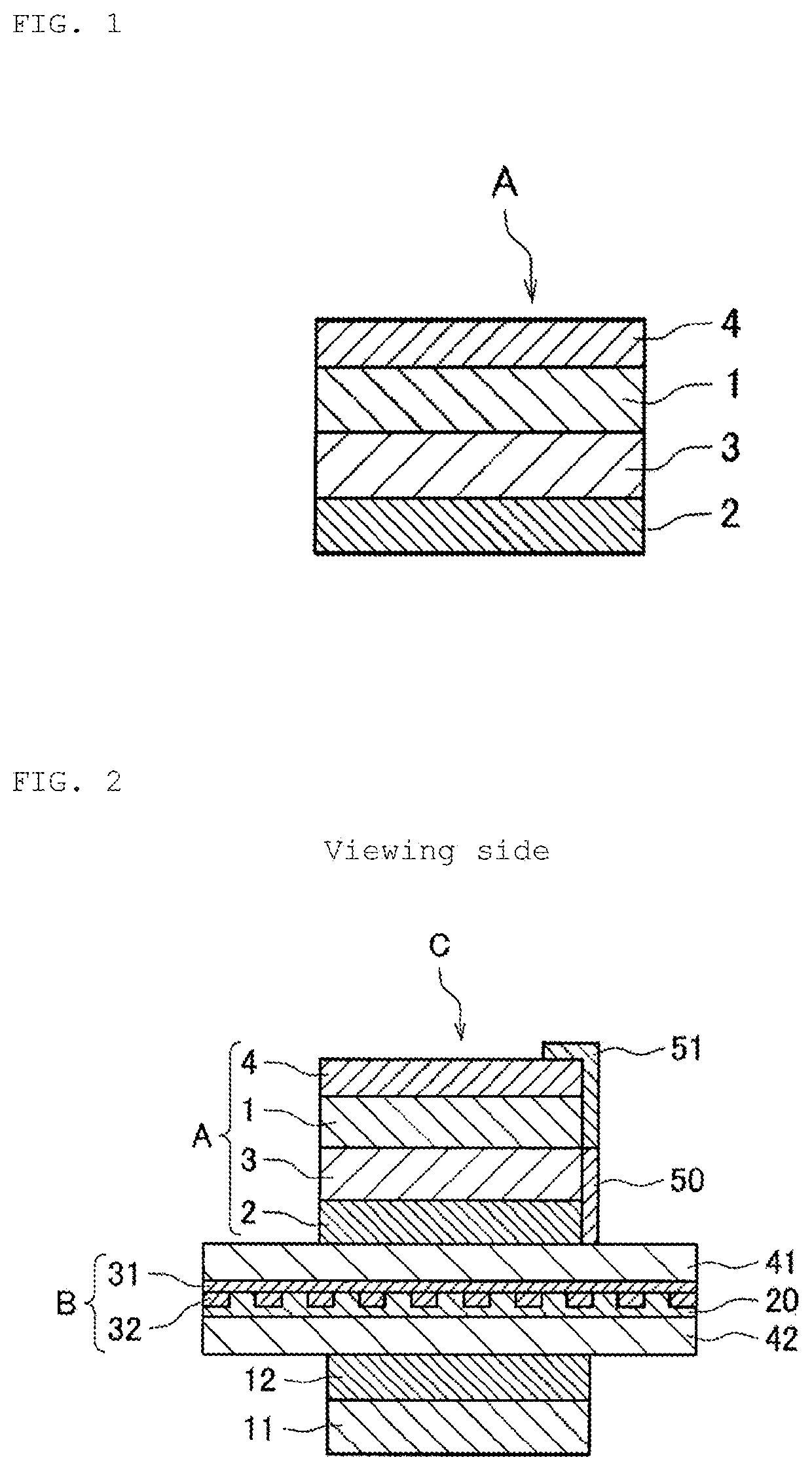
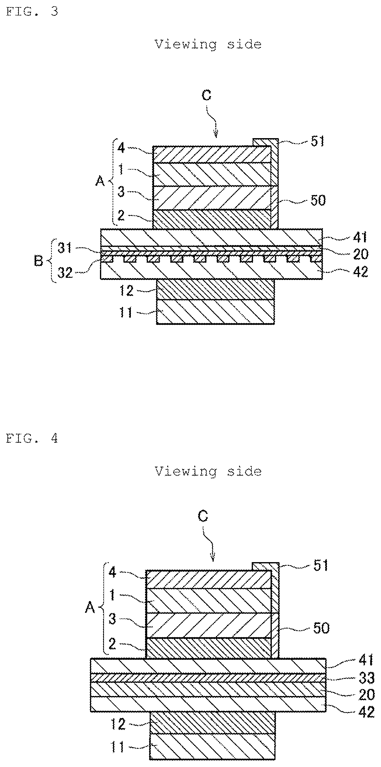
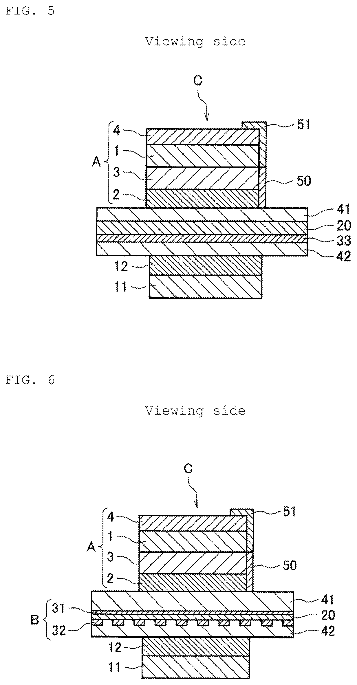
- Description
- Claims
- Application Information
AI Technical Summary
Benefits of technology
Problems solved by technology
Method used
Image

Examples
examples
[0108]Although the present invention will be described in detail below based on Production Examples and Examples, it should be understood that the present invention is not limited to such Examples. The parts and percentages in each Example are on a weight basis. Room temperature standing conditions not specified below are all 23° C. and 65% RH.
[0109]The weight average molecular weight (Mw) of the (meth)acrylic polymer was measured by GPC (gel permeation chromatography). The ratio Mw / Mn was also measured in the same manner.
[0110]Analyzer: HLC-8120 GPC, manufactured by Tosoh Corporation
[0111]Column: G7000HXL+GMHXL+GMHXL, manufactured by Tosoh Corporation
[0112]Column size: 7.8 mm φ×30 cm each in total 90 cm
[0113]Column temperature: 40° C.
[0114]Flow rate: 0.8 mL / min
[0115]Injection volume: 100 μL
[0116]Eluent: Tetrahydrofuran
[0117]Detector: Differential refractometer (RI)
[0118]Standard sample: Polystyrene
(Preparation of Polarizing Film)
[0119]An 80 μm-thick polyvinyl alcohol film was stret...
PUM
| Property | Measurement | Unit |
|---|---|---|
| Electrical resistance | aaaaa | aaaaa |
| Electrical resistance | aaaaa | aaaaa |
| Mass | aaaaa | aaaaa |
Abstract
Description
Claims
Application Information
 - Generate Ideas
- Intellectual Property
- Life Sciences
- Materials
- Tech Scout
- Unparalleled Data Quality
- Higher Quality Content
- 60% Fewer Hallucinations
Browse by: Latest US Patents, China's latest patents, Technical Efficacy Thesaurus, Application Domain, Technology Topic, Popular Technical Reports.
© 2025 PatSnap. All rights reserved.Legal|Privacy policy|Modern Slavery Act Transparency Statement|Sitemap|About US| Contact US: help@patsnap.com