Reduced instruction set processor based on memristor

a technology of instruction set and processor, applied in the field of computer processors, can solve the problems of frequent and costly data movement, and the bottleneck of von neumann, which will inevitably become the biggest obstacle limiting the performance of the computer, so as to improve the instruction processing speed, save power consumption, and avoid large power consumption and time consumption.

Pending Publication Date: 2021-04-22
HUAZHONG UNIV OF SCI & TECH
View PDF3 Cites 0 Cited by
  • Summary
  • Abstract
  • Description
  • Claims
  • Application Information

AI Technical Summary

Benefits of technology

[0014]The disclosure also provides a multi-chip parallel architecture processor based on a memristor, which includes a main chip and a total of Z computing chips. The main chip is used for memory, instruction processing, and task allocation, and is divided into a data region, an instruction region, and an instruction buffer. The computing chip is used for computation and the computing chip only includes an assistive region. There is a data path existed between the main chip and the computing chip. Data is transmitted between the main chip and the computing chip through the data path. Under the multi-chip parallel architecture, the instruction fetching, decoding, and address selection are serially executed one by one, the data is transmitted between the main chip and the computing chip through the data path, and the process of each computing chip executing a computing task may be performed in parallel. Therefore, the multi-chip parallel architecture can effectively improve the instruction processing speed.
[0015]Through the above technical solution conceived by the disclosure, compared with the architecture of memory and computation separation of modern computers, due to the memory and computation fusion characteristic and the in-situ computation characteristic of the reduced instruction set processor based on a memristor, the data in the chip may be directly calculated in situ through the implication operation while the data is stored in the chip. Therefore, there is no large power consumption and time spending caused by the continuous movement of data between the memory and the processor, so as to effectively achieve the beneficial effects of saving power consumption and shortening processing time.

Problems solved by technology

Such spending includes power consumption, time, space, etc.
Such frequent and costly data movement is considered as the “von Neumann bottleneck”.
It is foreseeable that as time goes by, the von Neumann bottleneck will inevitably become the biggest obstacle limiting the performance of the computer.

Method used


Image

  • Reduced instruction set processor based on memristor
  • Reduced instruction set processor based on memristor
  • Reduced instruction set processor based on memristor

Examples


embodiment 1

[0075]The operation sequence of Embodiment 1 is as follows, and before the operation starts, all bit line switches and connection switches are in the turned off state by default:

[0076](1.1) The row selection module selects the 6 CMUs of the corresponding addresses, and sets all the selected bits p thereof to 1.

[0077](1.2) One round of marking of position bits is performed:

CMUc1c2v1v2A10101A20110A31001A41010A50000A60011

[0078](1.3) The connection switch connects A1 and A2, connects A3 and A4, and A5 and A6 are not connected to any unit according to the values of the connection bits c1 and c2. The column selection module cooperates with the row selection module to turn on the 11-0 bits of bit line switches of A1 and A2, turn on all the 32 bits of bit line switches of A3 and A4, and turn on the 31-16 bits of line switches of A5.

[0079](1.4) After the voltage supply module finds all the units with p=1, the voltage supply module applies the voltage VCOND to A1 and A3, the voltage VSET to A...

embodiment 2

[0090]The operation sequence of Embodiment 2 is as follows, and before the operation starts, all bit line switches and connection switches are in the turned off state by default:

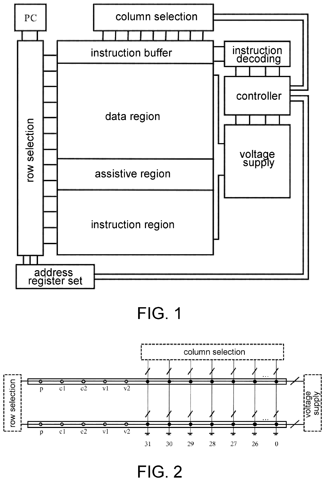
[0091](2.1) the row selection module selects a CMU (which is recorded as a unit A for convenience of description) with the on-chip address 0x31D, an assistive unit MOV1 of the assistive region data movement assistive block, and an instruction buffer (which is recorded as a unit I for convenience of description) with the address 0x000 according to the value in the program counter, and sets all the selected bits p thereof to 1.

[0092](2.2) One round of marking of position bits is performed:

CMUc1c2v1v2A0011MOV10000I0000

[0093](2.3) The column selection module cooperates with the row selection module to turn on all the 32 bits of bit line switches of MOV1 and I.

[0094](2.4) The voltage supply module applies the voltage VCLEAR to MOV1 and I according to the values of v1 and v2, so as to implement concurrent clear 0 ...

example 6

[0140] branch instruction if equal immediate “beqi, R1, R2, #x001”. Assuming that R1=0x3FD and R2=0x10C, sign extension to 32 bits is performed on the immediate #0x001, which is then compared with the data in the CMU with the address 0x10C pointed to by the source address register R2. If equal, the next instruction jumps to the instruction in the CMU with the address 0x3FD pointed to by the destination address register R1, and it is assumed that the data in the CMU with the address 0x10C is 0x0000001.

[0141]The implementation steps are as follows:

[0142](6.1) The instruction is fetched. Refer to the operation step for the instruction fetching in Example 2.

[0143](6.2) After the instruction is decoded, the row selection module selects the on-chip address 0x3FD (which is recorded as a unit A1 for convenience of description) and the on-chip address 0x10C (which is recorded as a unit A2 for ease of description), and the addresses of the assistive units BEQI0 to BEQI1 in the assistive block...


PUM


Abstract

A reduced instruction set processor based on a memristor is provided. The memristor is a non-volatile device using a resistor to store “0” and “1” logic while implementing “implication logic” through applying a pair of voltages VCOND/VSET. Various data operations, logic operations, and arithmetic operations may be implemented based on the implication logic. The memristor is a computation and memory fusion device having great potential. A computer processor based on the memristor also becomes the research direction of the next-generation computer processor. The computer processor based on a memristor is designed according to the memory and computation fusion characteristic of the memristor. The processor is different from a traditional computer that must use a special memory and a calculator, and fuses computation and memory. Compared with a traditional computer, the speed, parallelism degree, and power consumption of the computer processor based on the memristor are greatly improved.

Description

BACKGROUNDTechnical Field[0001]The disclosure relates to the field of computer processors, and particularly relates to a reduced instruction set processor based on a memristor.Description of Related Art[0002]All modern computers follow the design principle of the von Neumann architecture. In such architecture, the computing and memory modules are separated and are connected via a bus. When the computer is running, instructions and data are continuously transported between the processor and the memory through the bus. However, when the computer is running, the spending used in moving the data between the processor and the memory system is far greater than the spending for the actual computation of the processor. Such spending includes power consumption, time, space, etc. Such frequent and costly data movement is considered as the “von Neumann bottleneck”. As long as the computer still adopts the von Neumann architecture, the von Neumann bottleneck will always exist. It is foreseeable...

Claims


Application Information

Patent Timeline
Patent Type & Authority Applications(United States)
IPC IPC(8): G06F9/30G06F9/355G06F9/38G11C13/00
CPCG06F9/3001G06F9/3557G06F9/3814G06F9/3013G06F9/30134G06F9/30054G11C13/0038G06F9/30029G06F9/3877G11C13/0026G11C13/0028G11C13/0007G06F9/30058G11C11/005G06F9/30145
Inventor LIU, QUNWANG, YEWANGMIAO, XIANGSHUILI, JIAN
Owner HUAZHONG UNIV OF SCI & TECH
Why Eureka
Try Eureka