Embedded-type transparent electrode substrate and method for manufacturing same

a transparent electrode substrate and embedded technology, applied in the direction of dielectric characteristics, insulating substrate metal adhesion improvement, circuit optical details, etc., can solve the problem of high production cost of indium, low production efficiency of transparent led using ito, and limitation of being used as high-performance and low-cost transparent electrode elements. , to achieve the effect of preventing an increase in haze of the transparent electrode substrate and reducing raw material costs

Active Publication Date: 2021-06-24
LG CHEM LTD
View PDF0 Cites 0 Cited by
  • Summary
  • Abstract
  • Description
  • Claims
  • Application Information

AI Technical Summary

Benefits of technology

[0010]According to the exemplary embodiment of the present application, the metal foil pattern is formed by using the low-cost metal foil, such that it is possible to reduce raw material costs when manufacturing the transparent electrode substrate. In particular, according to the exemplary embodiment of the present application, the metal foil pattern is formed on the bonding layer, and then the heat treatment is performed at a temperature of 70° C. to 100° C., such that the embedded transparent electrode substrate in which the metal foil pattern is embedded in the bonding layer may be manufactured without a process of applying a separate pressure.
[0011]In addition, according to the exemplary embodiment of the present application, the metal foil pattern is formed on the bonding layer, and then the heat treatment is performed at a temperature of 70° C. to 100° C., such that it is possible to prevent an increase in haze of the transparent electrode substrate in accordance with illumination intensity of a surface of the metal foil.

Problems solved by technology

Indium is a main material of the ITO transparent electrode, but the amount of indium reserves is not available globally, and indium is produced only in some countries such as China, such that production cost of indium is high.
In addition, there is a disadvantage in that the displayed LED light is not constant because a resistance value is not constantly applied.
For this reason, the transparent LED using the ITO has a limitation in being used as a high-performance and low-cost transparent electrode element.
The ITO as a transparent electrode material has been the most widely used but has a limitation in terms of economic feasibility, limited performances, and the like, and as a result, researches and technology development using new materials are being continuously carried out.

Method used


Image

  • Embedded-type transparent electrode substrate and method for manufacturing same
  • Embedded-type transparent electrode substrate and method for manufacturing same
  • Embedded-type transparent electrode substrate and method for manufacturing same

Examples


example 1

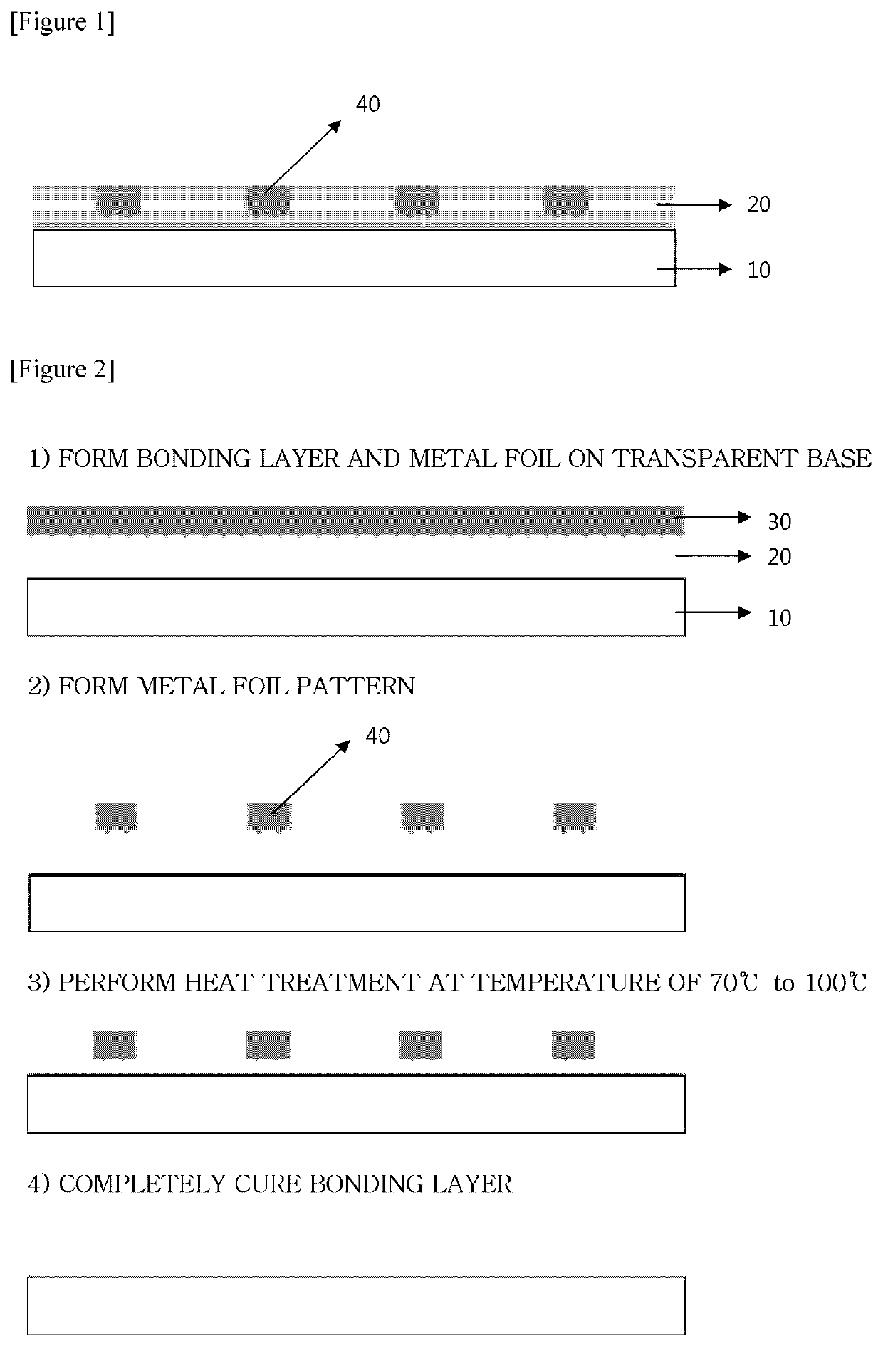
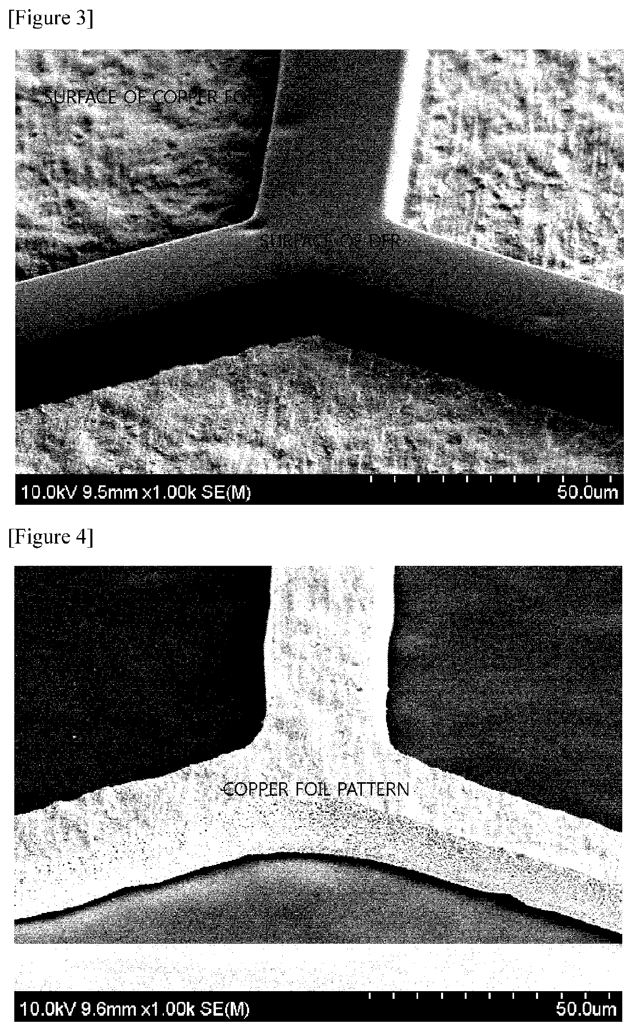
[0056]A UV-curable bonding agent was applied onto a PET film having a thickness of 250 μm by using a comma coater and then dried with hot blast at 100° C. for 5 minutes to form a bonding layer having a thickness of 15 μm. In this case, the UV-curable bonding agent comprised silane-modified epoxy resin KSR-277HMC70 (Kukdo Chemical) of 33 wt. %, silane-modified epoxy resin KSR-177 (Kukdo Chemical) of 35 wt. %, bisphenol A-type phenoxy resin YP-50E (Kukdo Chemical) of 30 wt. %, a positive ion initiator Irgacure 290 (BASF) of 1 wt. %, and a silane coupling agent KBM-403 (Shinetsu) of 1 wt. %.

[0057]The PET film having the transparent bonding layer and a copper foil having a thickness of 8 μm were hot-roll-laminated under a condition of 100° C. and 1.3 mpm (meter per minute).

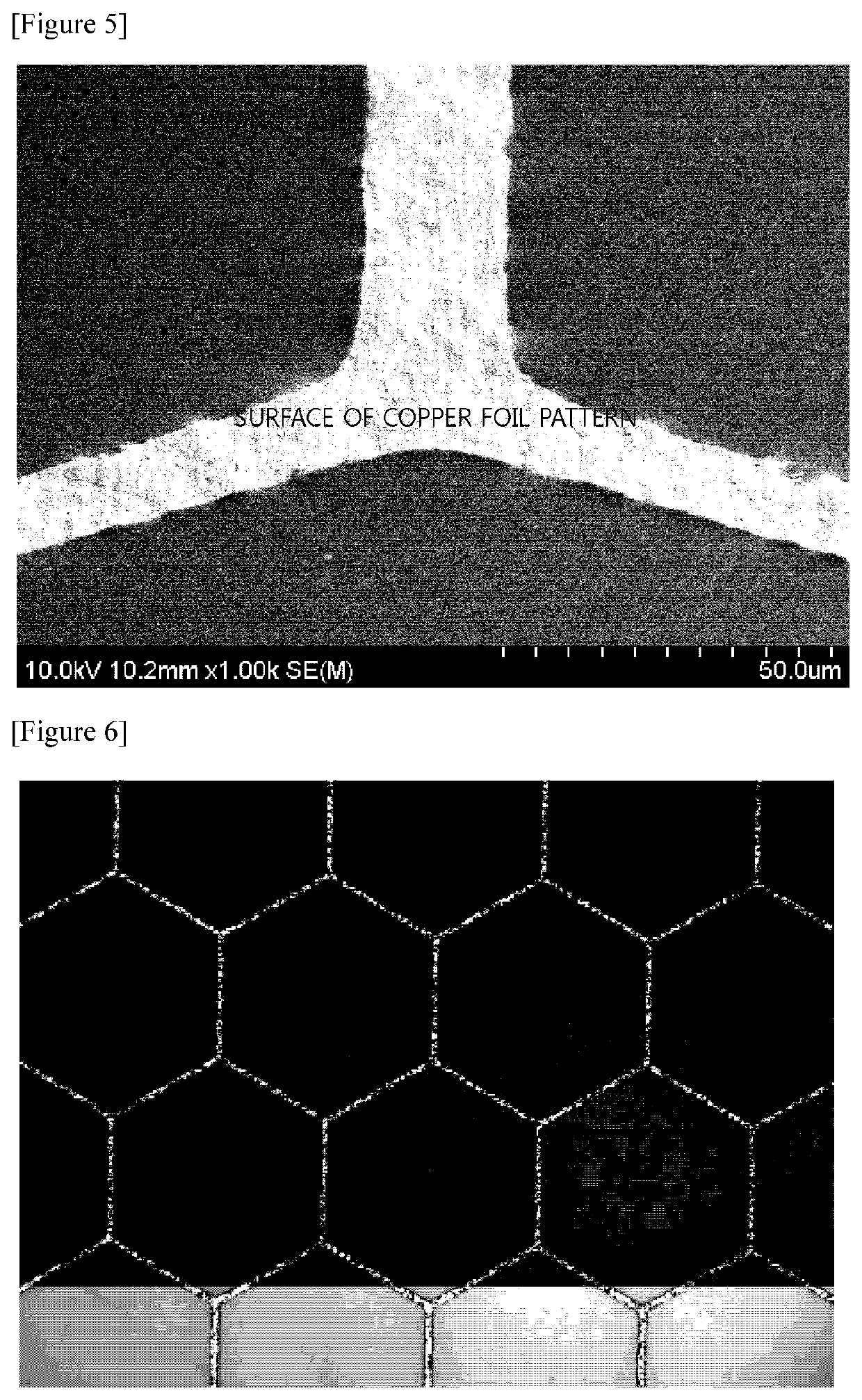
[0058]A dry film resist (DFR) was laminated on a surface of the copper foil of the copper-foil-laminated film, and then a hexagonal DFR pattern having a line width of 20 μm was formed through exposure and development ...


PUM

PropertyMeasurementUnit
temperatureaaaaaaaaaa
average roughness Rzaaaaaaaaaa

Abstract

A method of manufacturing a transparent electrode substrate according to an exemplary embodiment includes: a) forming a structure including a transparent base, a bonding layer on a surface of the transparent base, and a metal foil on a surface of the bonding layer opposite the transparent base; b) forming a metal foil pattern by patterning the metal foil; c) heat-treating the structure resulting from b) at a temperature of 70° C. to 100° C.; and d) completely curing the bonding layer. Also, a transparent electrode substrate is disclosed.

Description

TECHNICAL FIELD[0001]This application claims priority to and the benefit of Korean Patent Application No. 10-2018-0029686 filed with the Korean Intellectual Property Office on Mar. 14, 2018, the entire contents of which are incorporated herein by reference.[0002]The present application relates to an embedded transparent electrode substrate and a method of manufacturing the same.BACKGROUND ART[0003]Recently, in Korea, information and spectacles are being provided to urban people by presenting various landscape lighting in parks and downtown areas as well as gorgeous signboards through fusion of cutting-edge ICT technologies and LED technologies. In particular, a transparent LED display made of an ITO transparent electrode material is formed by applying an LED between sheets of glass or attaching a transparent film, to which the LED is applied, to one surface of glass. There is an advantage in that a luxurious appearance may be produced because no electric wire is visible. As a result...

Claims


Application Information

Patent Timeline
Patent Type & Authority Applications(United States)
IPC IPC(8): H05K3/38H05K1/02
CPCH05K3/386H05K3/389H05K3/067H05K2203/1453H05K1/0274H01L33/42H01L31/0224H01B13/00H01L25/0753H01B13/0026H01B13/0016H01L31/022466H05K2201/0108
Inventor SON, YONG GOOLEE, KUN SEOKMOON, JUNG OKLEE, KISEOKLEE, SEUNG HEON
Owner LG CHEM LTD
Why Eureka
Try Eureka