Mask pattern, semiconductor structure and fabrication method thereof

Active Publication Date: 2021-07-08
SEMICONDUCTOR MANUFACTURING INTERNATIONAL (BEIJING) CORP +1
View PDF0 Cites 0 Cited by
  • Summary
  • Abstract
  • Description
  • Claims
  • Application Information

AI Technical Summary

Benefits of technology

The patent provides a mask pattern that can create devices with both large and small critical dimensions. It achieves this through a two-step process. The first mask pattern is designed to make a single exposure and etching, while the second mask pattern takes advantage of a self-aligned process. By partially overlapping target patterns, the space is fully utilized and the pattern density of the second mask pattern is achieved without compromising the pattern density of the first mask pattern.

Problems solved by technology

However, in a case where both large and small critical dimensions need to be formed at the same time, when designing the mask pattern, the pattern density is not enough to meet the requirements of forming the device with a substantially small critical dimension.

Method used


Image

  • Mask pattern, semiconductor structure and fabrication method thereof
  • Mask pattern, semiconductor structure and fabrication method thereof
  • Mask pattern, semiconductor structure and fabrication method thereof

Examples


Embodiment Construction

[0038]Reference will now be made in detail to exemplary embodiments of the disclosure, which are illustrated in the accompanying drawings. Wherever possible, the same reference numbers will be used throughout the drawings to refer to the same or the alike parts.

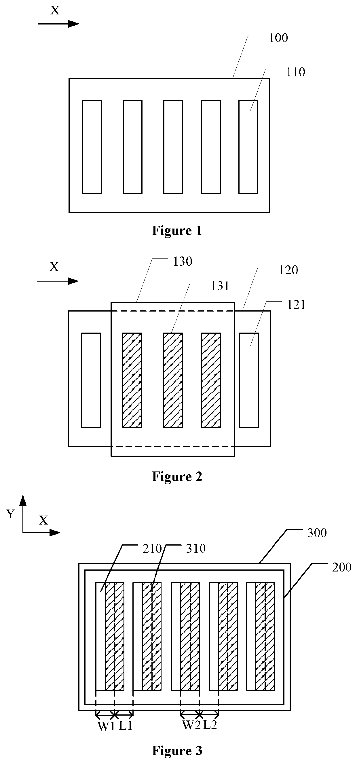
[0039]FIG. 1 illustrates a schematic structural diagram of a mask pattern. Referring to FIG. 1, a mask pattern 100 includes a plurality of first target patterns 110, and the plurality of first target patterns 110 are arranged along a first direction X.

[0040]The mask pattern 100 is used to perform a single exposure process and a single etching process, to form a device with a substantially large feature dimension. To simultaneously form a device with a substantially small feature dimension, another mask pattern is designed on the basis of the mask pattern 100, which will be described in detail below in conjunction with the accompanying drawings.

[0041]FIG. 2 illustrates a schematic structural diagram of another mask pattern. Re...


PUM


Abstract

A mask pattern, a semiconductor structure and a method for forming the semiconductor structure are provided. The mask pattern includes a first mask pattern and a second mask pattern. The first mask pattern includes a plurality of first target patterns, and the plurality of first target patterns are arranged along a first direction. The second mask pattern includes a plurality of second target patterns, and the plurality of second target patterns are arranged along the first direction. When the first mask pattern overlaps the second mask pattern, one of the plurality of first target patterns partially overlaps a corresponding one of the plurality of second target patterns.

Description

CROSS-REFERENCE TO RELATED APPLICATIONS[0001]This application claims the priority of Chinese patent application No. 202010010444.9, filed on Jan. 6, 2020, the entirety of which is incorporated herein by reference.FIELD OF THE DISCLOSURE[0002]The present disclosure generally relates to the field of semiconductor manufacturing technology and, more particularly, relates to a mask pattern, a semiconductor structure and a fabrication method thereof.BACKGROUND[0003]With the development of very large-scale integrated circuits, device design dimensions are getting smaller and smaller, and changes in device critical dimensions (CD) have more and more influence on device performance. For example, change in critical dimensions of a gate structure directly leads to changes in device operating speed.[0004]Photolithography is vital technology in semiconductor manufacturing technology. Photolithography can achieve the transfer of a pattern from a mask to a surface of silicon wafer, to form a semic...

Claims


Application Information

Patent Timeline
IPC IPC(8): H01L21/027H01L21/033H01L21/311G03F1/70
CPCH01L21/0274G03F1/70H01L21/31144H01L21/0337H01L21/0338G03F1/76G03F7/0035G03F1/00G03F1/36
Inventor SHU, QIANGZHANG, YINGCHUNQIN, LIUSHA
Owner SEMICONDUCTOR MANUFACTURING INTERNATIONAL (BEIJING) CORP
Why Eureka
Try Eureka