Thin-film white LED chip

a white led chip and thin film technology, applied in the field of thin film white led chips, can solve the problems of only down-converting the energy of photons of phosphorescent/fluorescent materials, affecting the overall efficiency of white led chips, and low external quantum efficiency of blue and ultraviolet leds, so as to improve external quantum efficiency, reduce lighting energy consumption, and reduce production costs

Pending Publication Date: 2021-09-16
SOUTH CHINA UNIV OF TECH
View PDF0 Cites 0 Cited by
  • Summary
  • Abstract
  • Description
  • Claims
  • Application Information

AI Technical Summary

Benefits of technology

[0009]An objective of the present invention is to provide a thin-film white LED chip, which significantl

Problems solved by technology

Moreover, the phosphorescent/fluorescent materials only down-convert the energy of the photons which can escape from the LED chip.
However, the external quantum efficiency of blue and ultraviolet LEDs is low, and the photoluminescence quantum efficiency of phosphorescent/fluorescent materials is generally less than 100%, which dramatically affects the overall efficiency of white LEDs (i.e. resulting in an even poorer efficiency of white LEDs based on the combination of electroluminescence and photoluminescence, compared with the original blue and ultraviolet LEDs).
In addition, for Strategy B, the strong ultraviolet emission is harmful to the human health, especially under long-term exposure.
Therefore, Strategy A, which uses blue LED chips to excite red/green (or yellow) phosphorescent/fluorescent materials based on the combination of electroluminescence and p

Method used


Image

  • Thin-film white LED chip
  • Thin-film white LED chip
  • Thin-film white LED chip

Examples


Embodiment Construction

[0038]The embodiments of the present invention will now be described with reference to the accompanying drawings. Similar element numbers in the accompanying drawings represent similar elements.

[0039]In order to explain in detail the technical content, construction features, the purpose and effect achieved by the present invention, the following combined with the implementation and the attached drawings are described in detail.

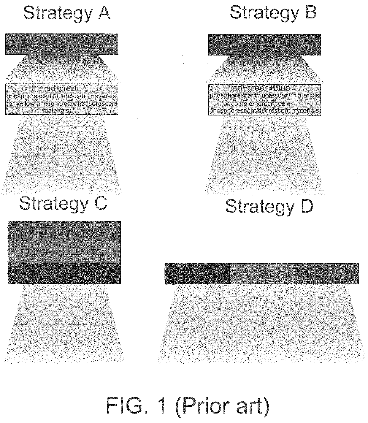
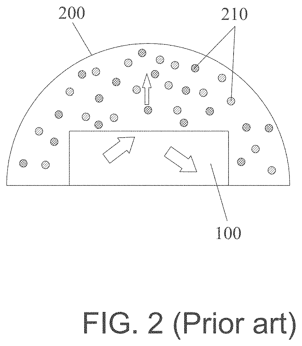
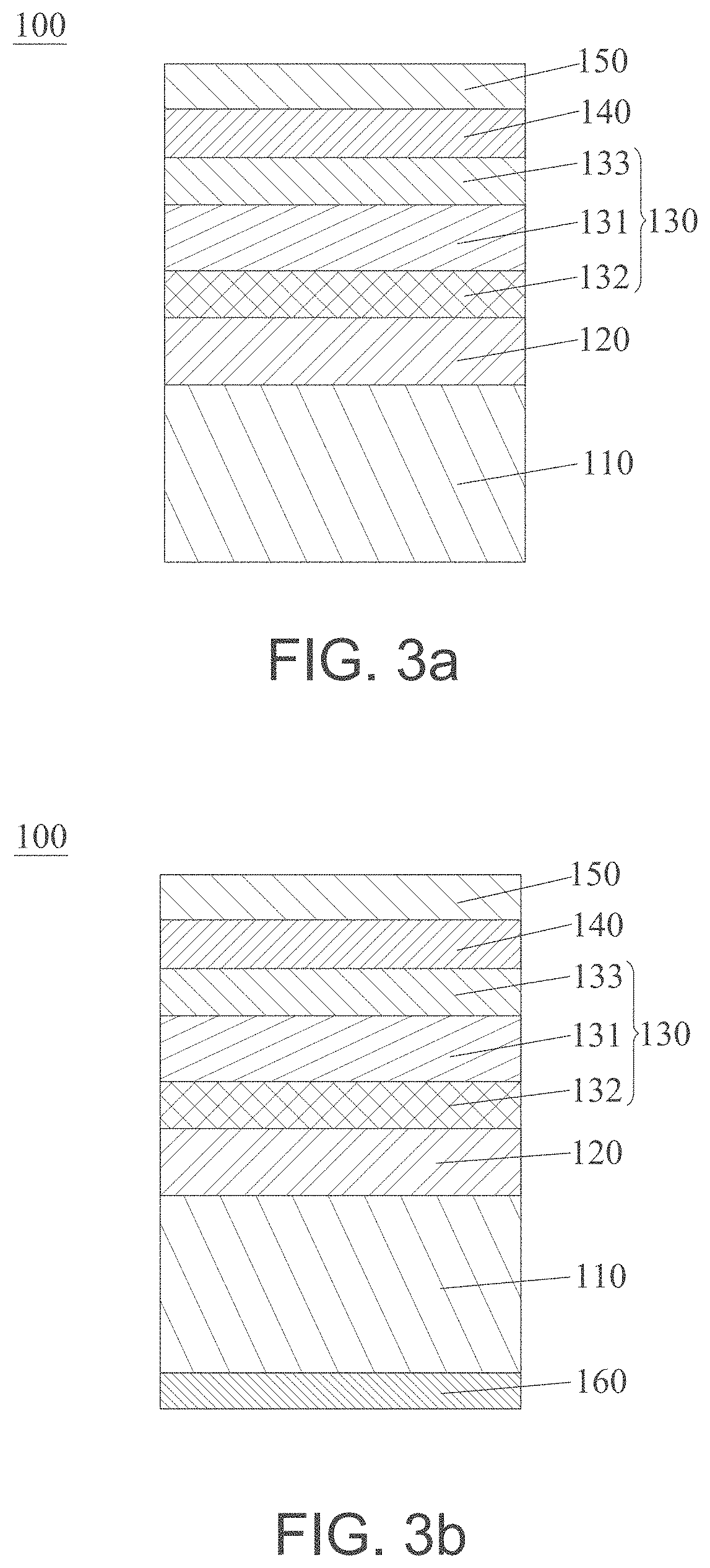
[0040]Referring to FIGS. 3a-4b, a thin-film white LED chip 100 of the present invention includes a transparent substrate 110, a first transparent electrode 120, an emissive structure 130, a second transparent electrode 140, and a first phosphorescent / fluorescent layer 150 respectively arranged in sequence. Specifically, in an inverted structure, the emissive structure 130 includes a emissive layer 131, an electron injection layer 133 and a hole injection layer 132 respectively formed at both sides of the emissive layer 131, and a total thickness of the electro...


PUM


Abstract

A thin-film white LED chip includes a transparent substrate, a first transparent electrode, an emissive structure, a second transparent electrode, and a first phosphorescent/fluorescent layer respectively arranged in sequence. The emissive structure includes an emissive layer, an electron injection layer and a hole injection layer respectively formed at both sides of the emissive layer, and a total thickness of the electron injection layer and the second transparent electrode (in an inverted structure) or a total thickness of the hole injection layer and the second transparent electrode (in a conventional structure) is smaller than a length of one emission wavelength of the emissive layer. The evanescent wave generated by total internal reflection can penetrate into and be absorbed by the first phosphorescent/fluorescent layer to further emit light, thereby the overall external quantum efficiency of the LED chip is improved.

Description

CROSS REFERENCE TO RELATED APPLICATIONS[0001]This application is a continuation-in-part application of International (PCT) Patent Application No. PCT / CN2020 / 071635, filed on Jan. 13, 2020. The contents of the above-identified application are incorporated herein by reference.FIELD OF THE INVENTION[0002]The present invention relates to technical field of light emitting diodes (LEDs), and in particular to a thin-film white LED chip with high external quantum efficiency and low production cost.BACKGROUND OF THE INVENTION[0003]White light illumination is closely related to people's work and lives, and white light illumination technology has already been greatly developed in the past several decades. Specifically, white LEDs have become one of the best alternatives to traditional lighting devices (such as incandescent lamps and fluorescent lamps), therefore, it is a mainstream to use the energy-saving and environmentally friendly white LEDs as the lighting devices nowadays. While the trad...

Claims


Application Information

Patent Timeline
IPC IPC(8): H01L33/42H01L33/48
CPCH01L33/42H01L33/486H01L33/38H01L33/505H10K50/00
Inventor CHEN, ZIMINGYE, XUANLILI, ZHENCHAOCAO, YONG
Owner SOUTH CHINA UNIV OF TECH
Why Eureka
Try Eureka