Check patentability & draft patents in minutes with Patsnap Eureka AI!

Imaging device based on colloidal quantum dots

Pending Publication Date: 2021-11-18
UNIVERSITY OF GRONINGEN
View PDF0 Cites 0 Cited by
  • Summary
  • Abstract
  • Description
  • Claims
  • Application Information

AI Technical Summary

Benefits of technology

The present patent is about an imaging device and a method of manufacturing it. The device comprises a stack of photoactive layers, which typically includes quantum dots formed by semiconductor nanocrystals capped by ligands. The layers can be made by depositing a solution with colloidal quantum dots. The device can be made without any inorganic matrix filling or barrier layers. The quantum dots can be deposited in a single processing step, which is faster than traditional methods. The photoactive layers can have different structures, and the device can be used for various imaging applications. The device includes pixels with corresponding readout electronics, which can amplify the photo-generated charges. The technical effects of this patent are faster and more efficient manufacturing of imaging devices with improved performance.

Problems solved by technology

These ligands effectively passivate the surface of the CQDs, which may result in low defect density and, therefore, low density of trap states within the band gap of the CQDs.
However, these systems may suffer from slow operation speed due to low mobility and long pathways for the carriers and relatively low quantum efficiency.
The material of the matrix can in principle provide n- or p-type doping of quantum dots, which however may lose photosensitivity due to high concentration of free charges and fast recombination of photo-generated charges.

Method used


Image

  • Imaging device based on colloidal quantum dots
  • Imaging device based on colloidal quantum dots
  • Imaging device based on colloidal quantum dots

Examples


Embodiment Construction

[0018]Terminology used for describing particular embodiments is not intended to be limiting of the invention. As used herein, the singular forms “a”, “an” and “the” are intended to include the plural forms as well, unless the context clearly indicates otherwise. The term “and / or” includes any and all combinations of one or more of the associated listed items. It will be understood that the terms “comprises” and / or “comprising” specify the presence of stated features but do not preclude the presence or addition of one or more other features. It will be further understood that when a particular step of a method is referred to as subsequent to another step, it can directly follow said other step or one or more intermediate steps may be carried out before carrying out the particular step, unless specified otherwise. Likewise it will be understood that when a connection between structures or components is described, this connection may be established directly or through intermediate stru...


PUM


Abstract

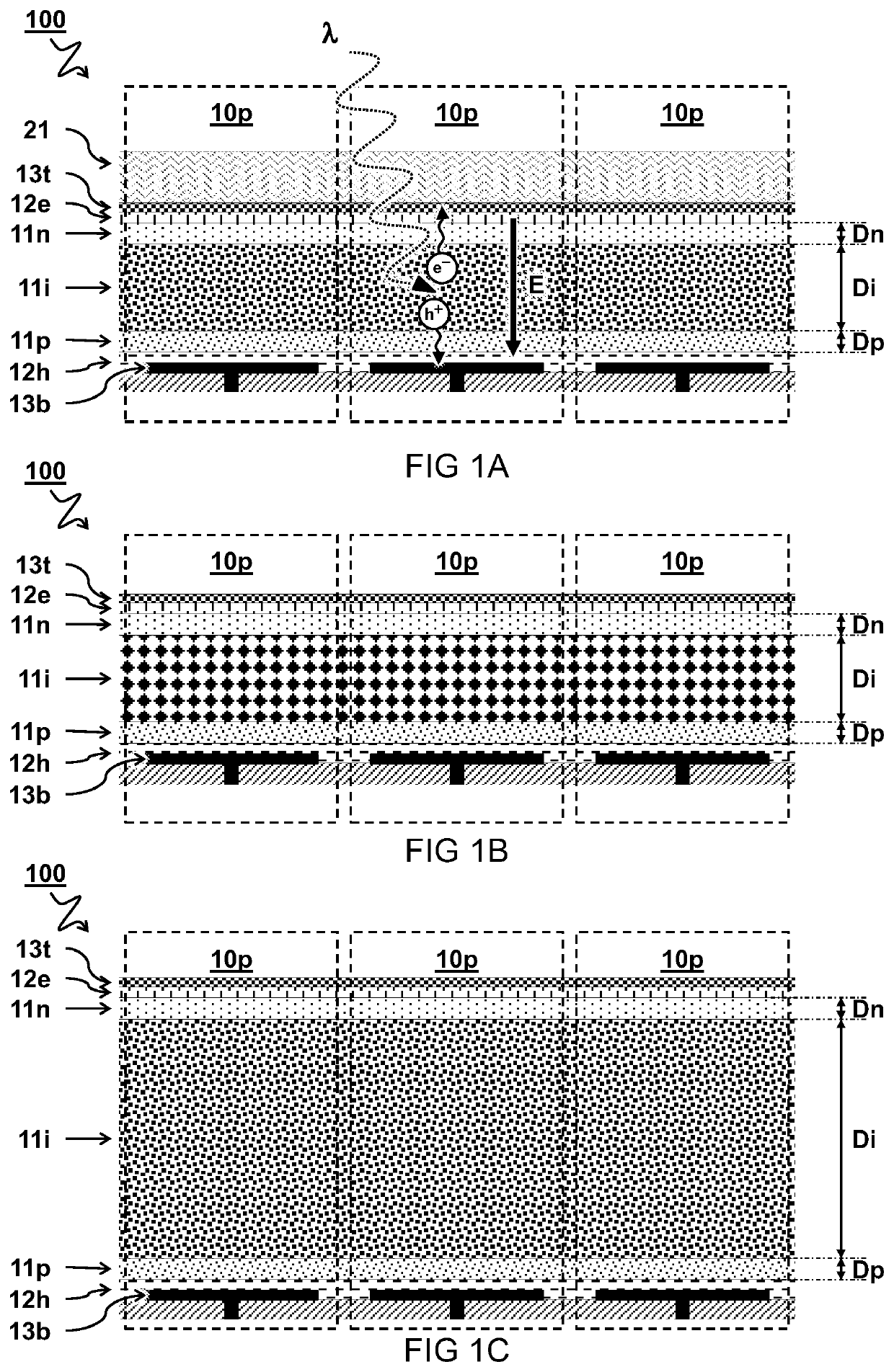
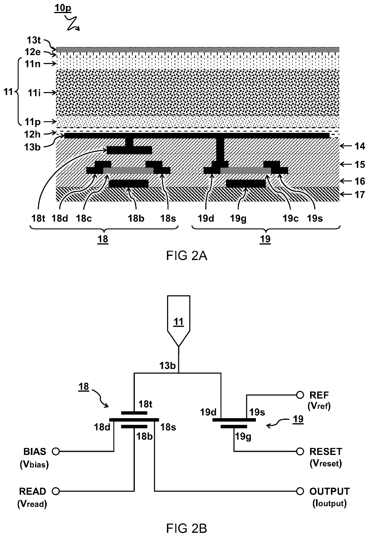
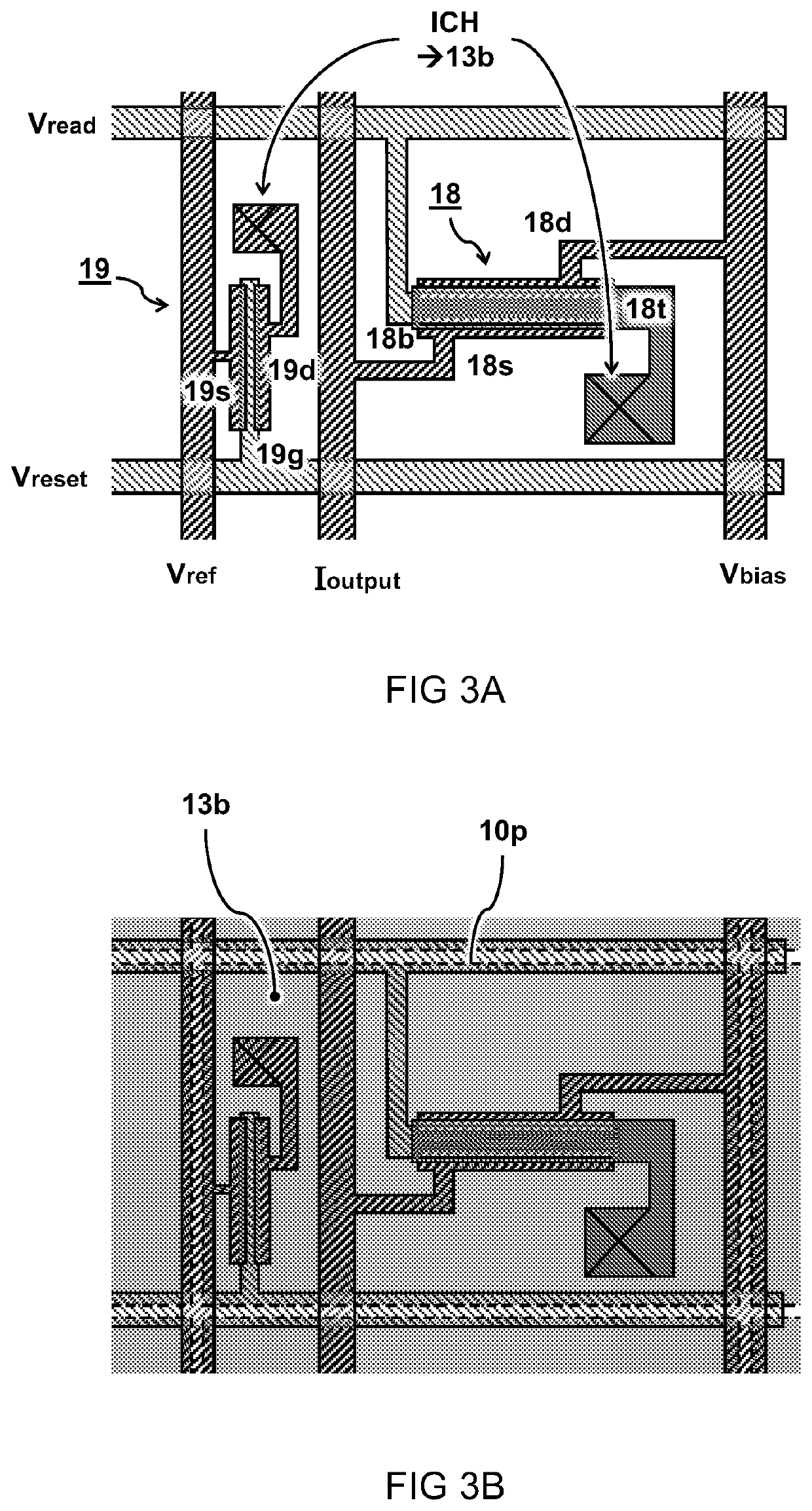
An imaging device (100) comprises a stack of photoactive layers (11) including at least a p-type photoactive layer (11p) and an n-type photoactive layer (11n). The photoactive layers comprise quantum dots (QD) formed by semiconductor nanocrystals capped by ligands. Readout electronics comprise electrodes (13t, 13b) sandwiching the photoactive layers (11). At least one of the electrodes (13b) is divided in respective pixels (10p) for collecting photo-generated charges from respective parts of the photoactive layers. Each pixel (10p) comprises an amplification circuit to amplify the photo-generated charge, preferably using a DG-FET. An intermediate layer (11i) can be provided between the p- and n-type photoactive layers (11p, 11n).

Description

TECHNICAL FIELD AND BACKGROUND[0001]Aspects of the present disclosure relate to an imaging device with photoactive layers comprising colloidal quantum dots (CQDs). Further aspects may relate to structure and fabrication methods for photodetectors and imaging sensors using CQDs and / or other thin film materials.[0002]Colloidal quantum dots typically comprise nanocrystals of inorganic material that have discrete energy levels due to quantum confinement of electrons within the volume of the nanoparticles. CQDs, synthesized from different materials, have size-dependent band gap that can be optimized for light absorption in the selected range of wavelengths. The material choice may be important for the size of the band gap, and for charge transport and absorption properties of the material. Advantages of CQDs may include high light absorption coefficient, high charge-carrier mobilities, solution-processability and low price. CQD films, casted on top of a virtually any substrate, can be fu...

Claims


Application Information

Patent Timeline
IPC IPC(8): H01L31/0352H01L27/146H04N5/369H04N5/378
CPCH01L31/035218H01L27/14614H04N5/378H04N5/379H01L27/14683H01L27/14601H01L31/101H04N25/75H04N25/79
Inventor SHULGA, ARTEM GENNADIIOVYCHLOI, MARIA ANTONIETTA
Owner UNIVERSITY OF GRONINGEN
Features
  • R&D
  • Intellectual Property
  • Life Sciences
  • Materials
  • Tech Scout
  • Unparalleled Data Quality
  • Higher Quality Content
  • 60% Fewer Hallucinations
Learn More