
Photoelectric conversion element

a conversion element and photoelectric technology, applied in the direction of capacitors, solid-state devices, electrolytic capacitors, etc., can solve the problems of difficult high-speed response, achieve the effect of enhancing response characteristics, reducing electric resistance, and upgrading the responsive speed of photoelectric conversion elements

Inactive Publication Date: 2018-08-30
NAGOYA UNIVERSITY +1
View PDF1 Cites 3 Cited by
  • Summary
  • Abstract
  • Description
  • Claims
  • Application Information

AI Technical Summary

Benefits of technology

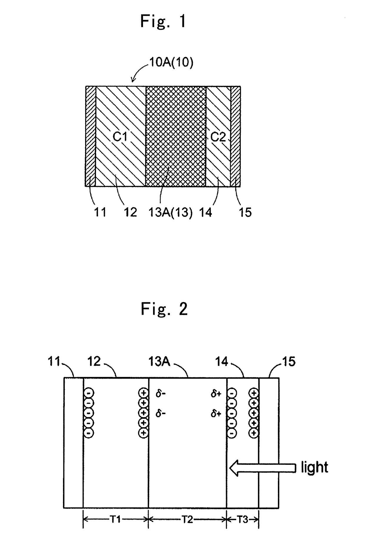
The patent describes a device that uses an organic semiconductor to convert light into electricity. The device has two layers of insulators with different capacitances. When the device is exposed to light, the first insulator becomes polarized and creates an electric field in the intermediate layer of the organic semiconductor, which further enhances the charge separation and improves the device's response speed. Additionally, the device has a conductor that helps decrease the electric resistance and improve the device's responsive speed. Overall, this device has improved performance compared to previous generations of organic photovoltaic devices.

Problems solved by technology

However, conventional photoelectric conversion elements, to which the technologies disclosed in Patent Literature No. 1 and Non-patent Literature Nos. 1 through 3 are applied, have been associated with the following problems.
First, the capacitance of the polarized layer can be enlarged in order to make a current flowing within a system, but the enlarging time constant makes it difficult to carry out a high-speed response.

Method used


Image

  • Photoelectric conversion element
  • Photoelectric conversion element
  • Photoelectric conversion element

Examples


first embodiment

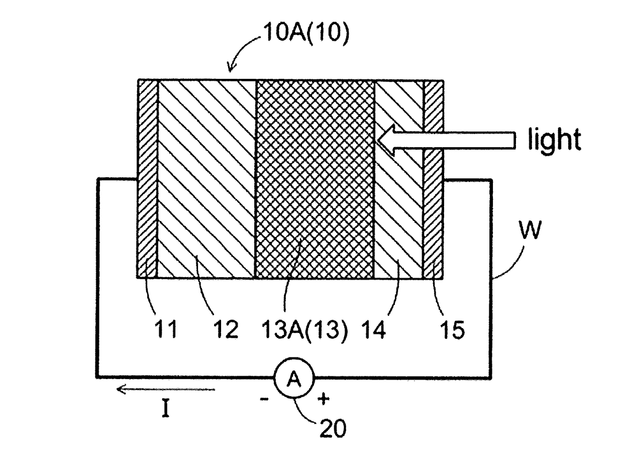
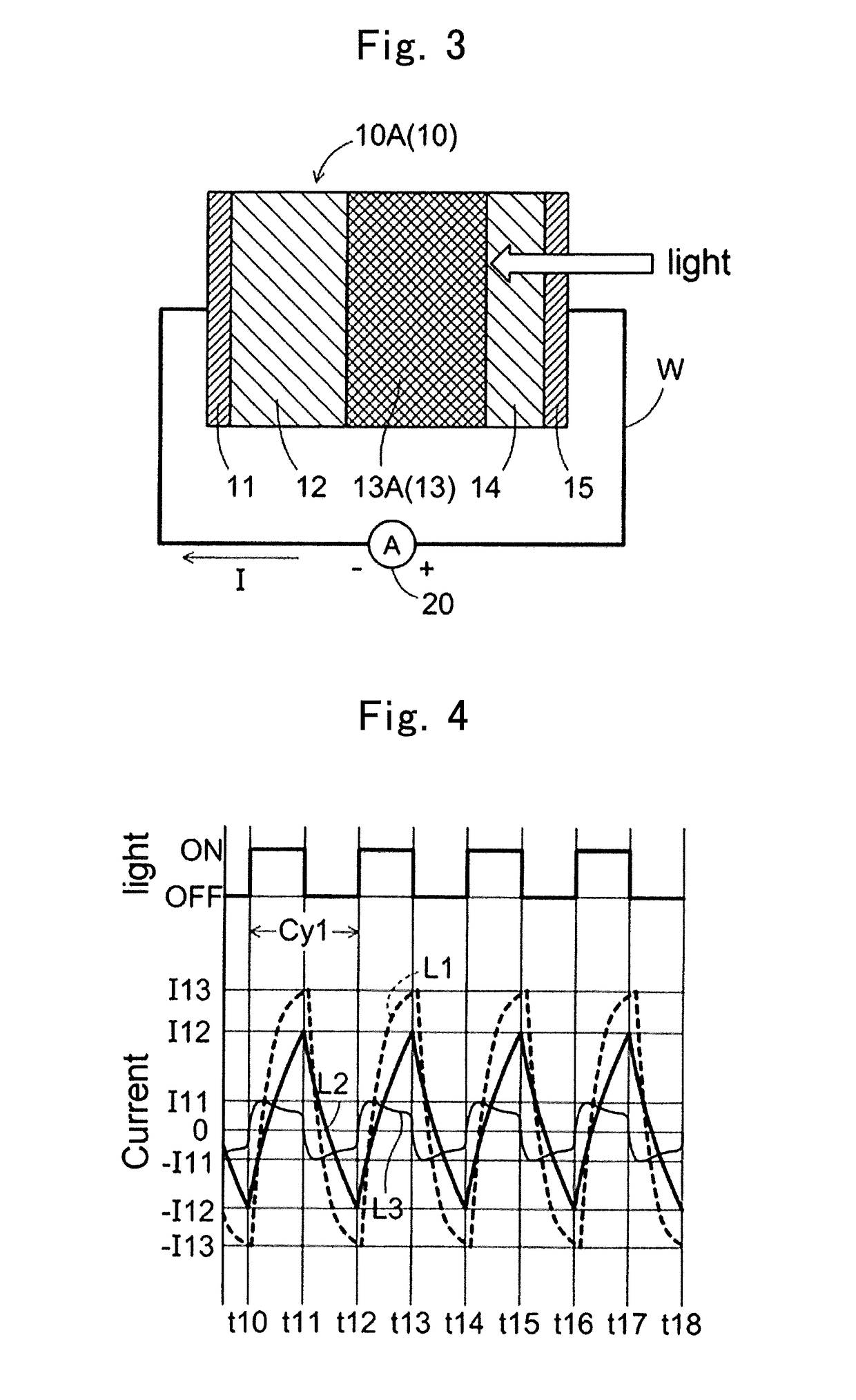
[0030]First Embodiment will be hereinafter described with reference to FIGS. 1 through 4. A photoelectric conversion element 10A is one of the examples or variations of a photoelectric conversion element 10. The photoelectric conversion element 10A comprises a first electrode 11, a first insulator 12, an organic semiconductor 13A, a second insulator 14, and a second electrode 15.

[0031]The first electrode 11 and second electrode 15 correspond to the claimed “a pair of electrodes.” It is not necessarily needed to use a transparent electrode, which exhibits optical transparency, for the first electrode 11 and second electrode 15 as far as they have an elemental structure capable of optically exciting the organic semiconductor 13A directly. However, when exciting the organic semiconductor 13A by way of one of the electrodes, the electrode is required to exhibit transparency. The following are exemplary materials for transparent electrically conducting member: tin oxide with antimony or ...

second embodiment

[0061]A photoelectric conversion element 10B according to Second Embodiment of the present invention will be hereinafter described with reference to FIGS. 5 and 6. Note that, in order to concisely illustrate and describe Second Embodiment, descriptions on the same constituents as those employed in First Embodiment will be omitted by designating them with identical reference numerals or symbols unless specified otherwise explicitly. Hence, descriptions on Second Embodiment will be hereinafter provided mainly regarding only the features that are distinct from those of First Embodiment.

[0062]The photoelectric conversion element 10B illustrated in FIG. 5 is one of the examples of the photoelectric conversion element 10. The photoelectric conversion element 10B comprises the first electrode 11, the first insulator 12, an organic semiconductor 13B, the second insulator 14, and the second electrode 15. The photoelectric conversion element 10B differs from the photoelectric conversion eleme...


PUM

PropertyMeasurementUnit
work functionsaaaaaaaaaa
dark currentaaaaaaaaaa
thicknessaaaaaaaaaa

Abstract

A photoelectric conversion element includes: a pair of electrodes including a first electrode and a second electrode; a first insulator having a first capacitance, and disposed to make contact with the first electrode; a second insulator having a second capacitance, which is smaller than the first capacitance of the first insulator, and disposed to make contact with the second electrode; and an organic semiconductor receiving a light to generate an electromotive force, and interposed between the first insulator and the second insulator to make contact with them.

Description

TECHNICAL FIELD[0001]The present invention relates to a photoelectric conversion element converting light energy into electric energy.BACKGROUND ART[0002]For example, Patent Literature No. 1 discloses an example of the conventional technologies for the purpose of providing a photoelectric conversion element with satisfactory photoelectric conversion efficiency and good optical response characteristics. The photoelectric conversion element comprises a photoelectric conversion layer including a charge-separated layer and a polarized layer. The charge-separated layer contains a semiconductor material in which the electron mobility and hole mobility differ on another, and a dopant having electron conductivity. The polarized layer is formed of an ionic liquid whose major components include a combination of a positive ion and negative ion.RELATED TECHNICAL LITERATUREPatent Literature[0003]Patent Literature No. 1: Japanese Unexamined Patent Publication (KOKAI) Gazette No. 2013-218924Non-Pa...

Claims


Application Information

Patent Timeline
Patent Type & Authority Applications(United States)
IPC IPC(8): H01L51/44H01L51/00
CPCH01L51/442H01L51/0047H01L51/0036H01G9/2013H10K39/30H10K85/311H10K30/451H10K30/354H10K2102/351Y02E10/549H10K30/82H10K30/352H10K30/353H10K85/113H10K85/215
Inventor AWAGA, KUNIODALGLEISH, SIMONREISSIG, LOUISAYUYAMA, KANAKO
Owner NAGOYA UNIVERSITY
Learn More