Wearable display device
- Summary
- Abstract
- Description
- Claims
- Application Information
AI Technical Summary
Benefits of technology
Problems solved by technology
Method used
Image
Examples
first embodiment
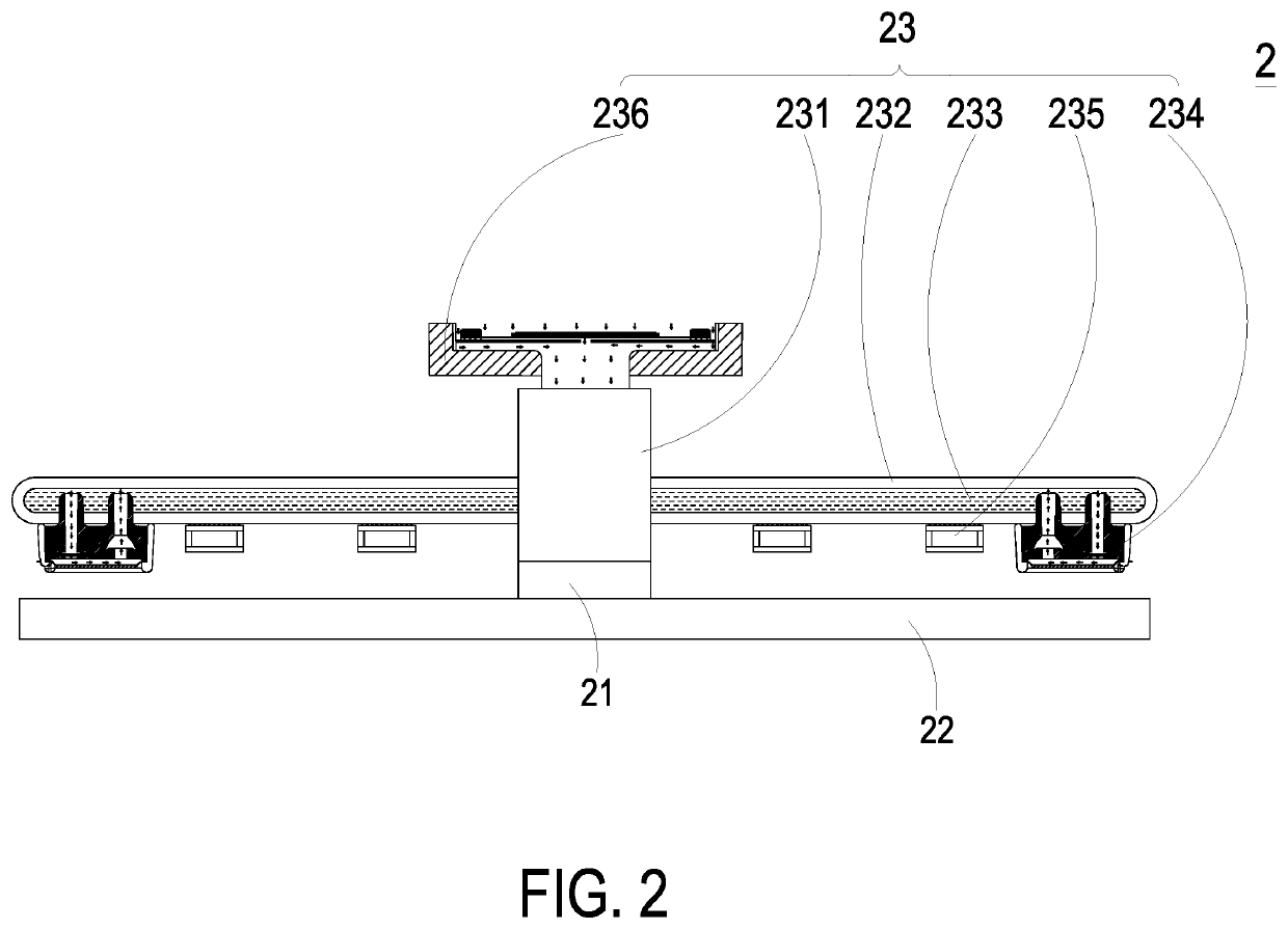
[0019]the micro pump 236 is shown in FIG. 4A to FIG. 4C. In the embodiment, the micro pump 236 is a microelectromechanical-system blower 3 and includes an outlet base 31, a first oxidation layer 32, a gas jetting resonance layer 33, a second oxidation layer 34, a resonance-chamber layer 35 and a first piezoelectric component 36, which are all manufactured by semiconductor process. In the embodiment, the semiconductor process includes at least one etching process and at least one deposition process. The etching process is one selected from the group consisting of a wet etching process, a dry etching process and a combination thereof, but not limited thereto. The deposition process is one selected from the group consisting of a physical vapor deposition process (PVD), a chemical vapor deposition process (CVD) and a combination thereof, and not redundantly described hereafter.
[0020]In the embodiment, the outlet base 31 includes an outlet chamber 311 and a compression chamber 312 formed...
second embodiment
[0022]the micro pump 236 is shown in FIG. 5A to FIG. 5C. In the embodiment, the micro pump 236 is a microelectromechanical-system pump 4. As shown in FIG. 5A, FIG. 5B and FIG. 5C, the microelectromechanical-system pump 4 includes an inlet base 41, a third oxidation layer 42, a resonance layer 43, a fourth oxidation layer 44, a vibration layer 45 and a second piezoelectric component 46, which are all manufactured by semiconductor process. In the embodiment, the semiconductor process includes at least one etching process and at least one deposition process. The etching process is one selected from the group consisting of a wet etching process, a dry etching process and a combination thereof, but not limited thereto. The deposition process is one selected from the group consisting of a physical vapor deposition process (PVD), a chemical vapor deposition process (CVD) and a combination thereof, and not redundantly described hereafter.
[0023]In the embodiment, the inlet base 41 includes a...
PUM
 Abstract
Description
Claims
Application Information


