

Integrated circuit (IC) package substrate with embedded trace substrate (ETS) layer on a substrate, and related fabrication methods
- Summary
- Abstract
- Description
- Claims
- Application Information
AI Technical Summary
Benefits of technology
Problems solved by technology
Method used
Image

Examples
Embodiment Construction
[0020]With reference now to the drawing figures, several exemplary aspects of the present disclosure are described. The word “exemplary” is used herein to mean “serving as an example, instance, or illustration.” Any aspect described herein as “exemplary” is not necessarily to be construed as preferred or advantageous over other aspects.
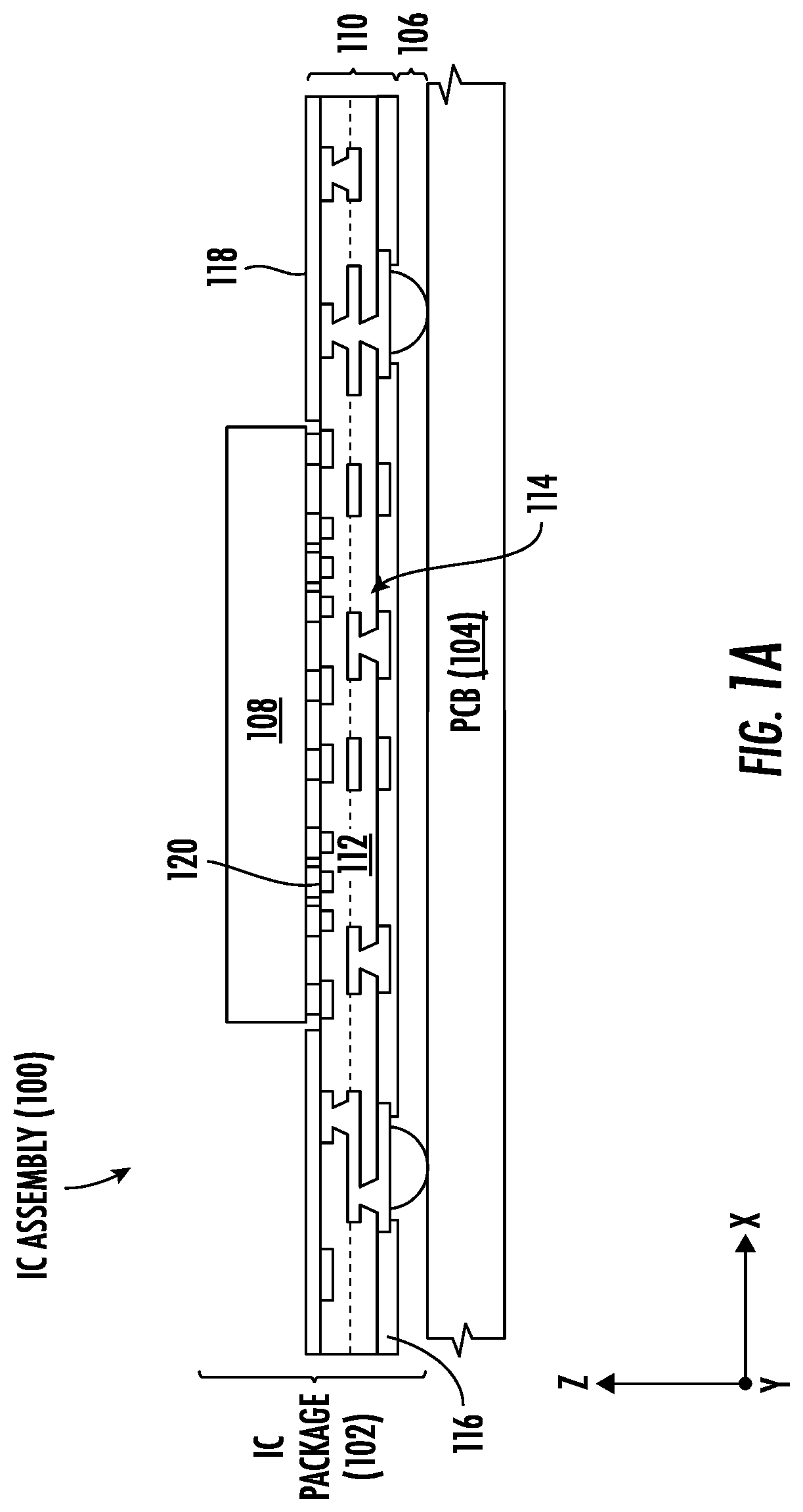
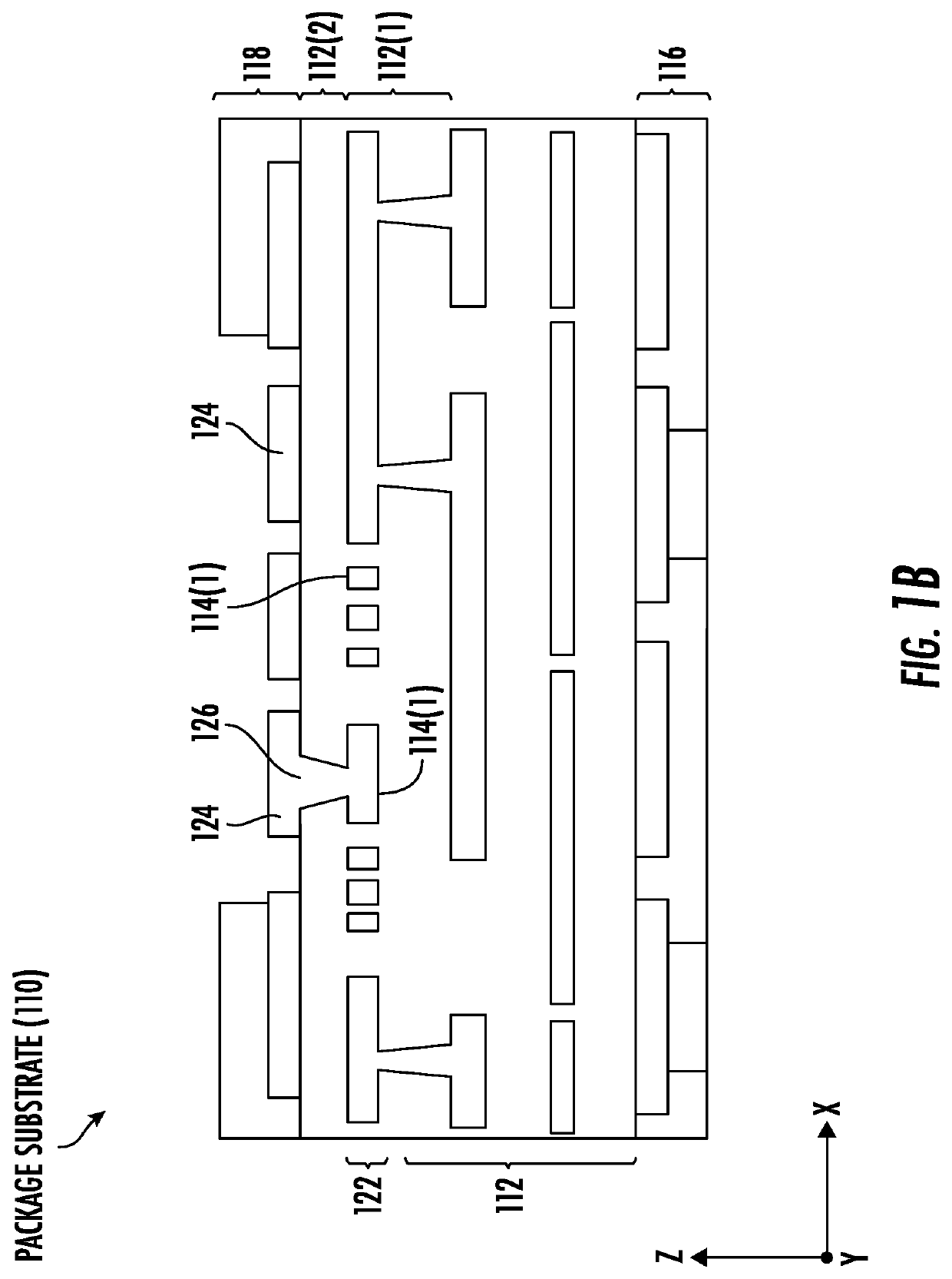
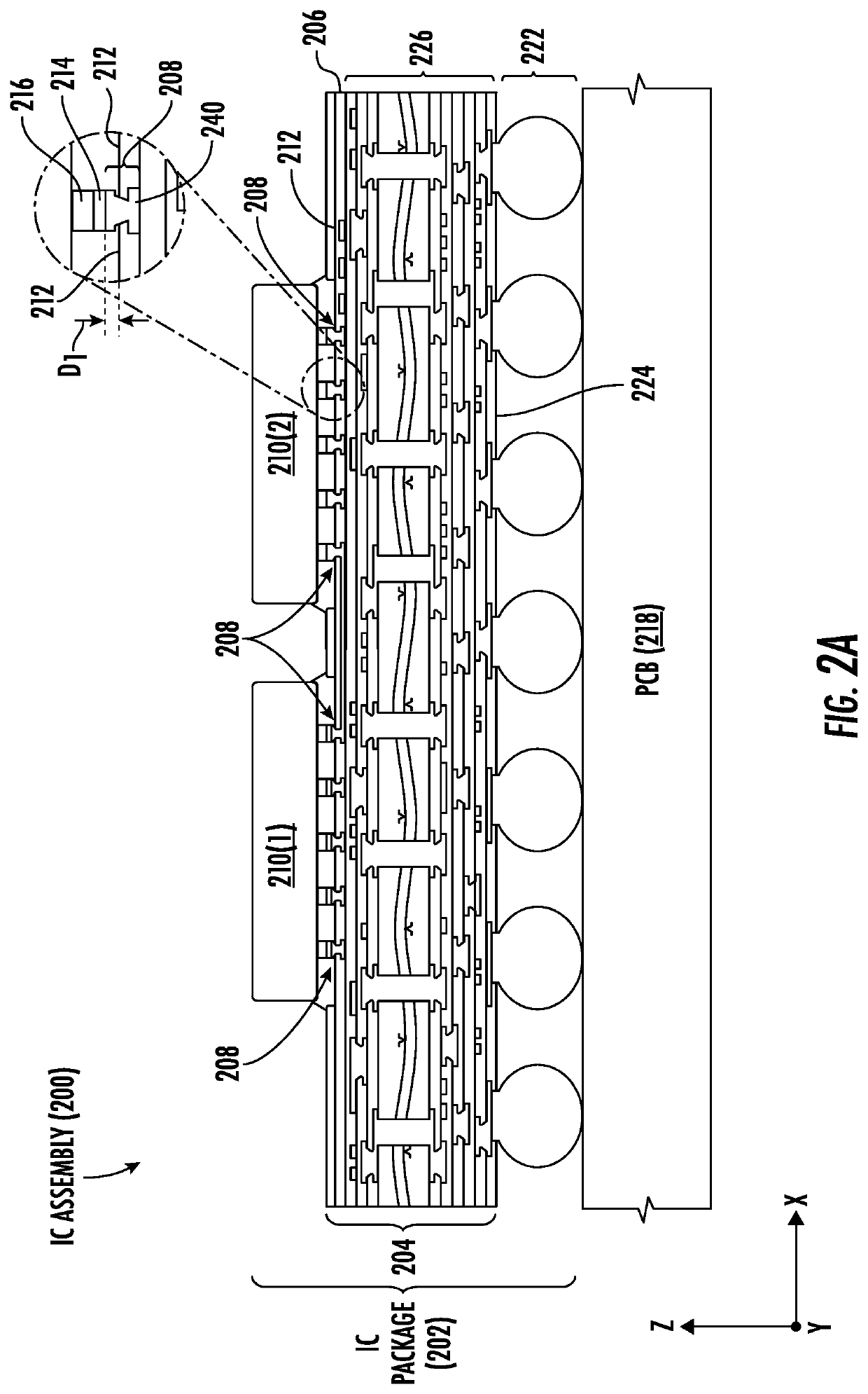
[0021]Aspects disclosed herein include integrated circuit (IC) package substrate with an embedded trace substrate (ETS) layer on a substrate. Related fabrication methods are also disclosed. The substrate can be a cored or coreless substrate. In exemplary aspects, a package substrate of the IC package includes an ETS layer disposed on the substrate to facilitate providing higher density ETS interconnects to provide bump / solder joints for coupling a semiconductor die (also referred to as “IC die” or “die”) to the package substrate. The ETS layer is a coreless structure that includes metal traces embedded in a dielectric material for signal routing. Meta...
PUM
 Abstract
Description
Claims
Application Information