
Multi-Sensing PTAT for Multiple-Location Temperature Sensing

a temperature sensing and multi-sensing technology, applied in the field of integrated circuits, can solve the problems of increasing circuit area and complexity, difficult to locate the sense device close to the desired location, and unnecessarily duplicate the control circuit(s) and the processing circuit(s), so as to reduce the leakage current

Active Publication Date: 2022-03-31
AYDEEKAY LLC DBA INDIE SEMICON
View PDF3 Cites 0 Cited by
  • Summary
  • Abstract
  • Description
  • Claims
  • Application Information

AI Technical Summary

Benefits of technology

The patent text describes a way to route signals in a bus, which can help to reduce congestion and leakage current. These signals can be routed together in common shielded groups, which can bring them closer to the controller without causing interference. Additionally, there is a signal line from temperature sensors to the controller, which helps to monitor and reduce temperature-related issues.

Problems solved by technology

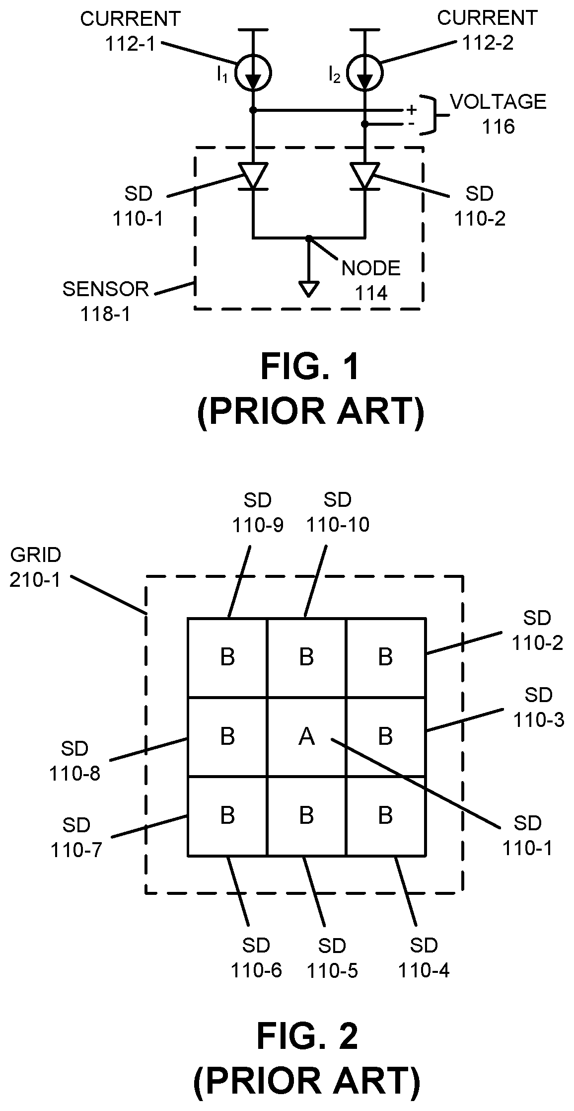
Furthermore, because the management techniques use the local temperature of the component being monitored, multiple components in a semiconductor die may require individual temperature monitoring when these components can be at different temperatures because of thermal non-uniformities across the semiconductor area.
Addressing these issued can result in increased circuit area and complexity, so that the implementation of a temperature sensor may be dominated by the control circuit(s) and processing circuit(s) and not the temperature sensor devices.
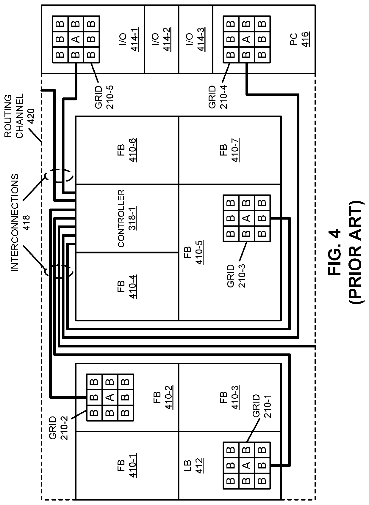
However, it can be difficult to locate the sense devices close to the desired location of the semiconductor surface to be measured because of constraint of having to also locate the control circuit(s) and the processing circuit(s) at that location.
Moreover, when multiple sensor devices are used, this approach unnecessarily duplicates the control circuit(s) and the processing circuit(s).
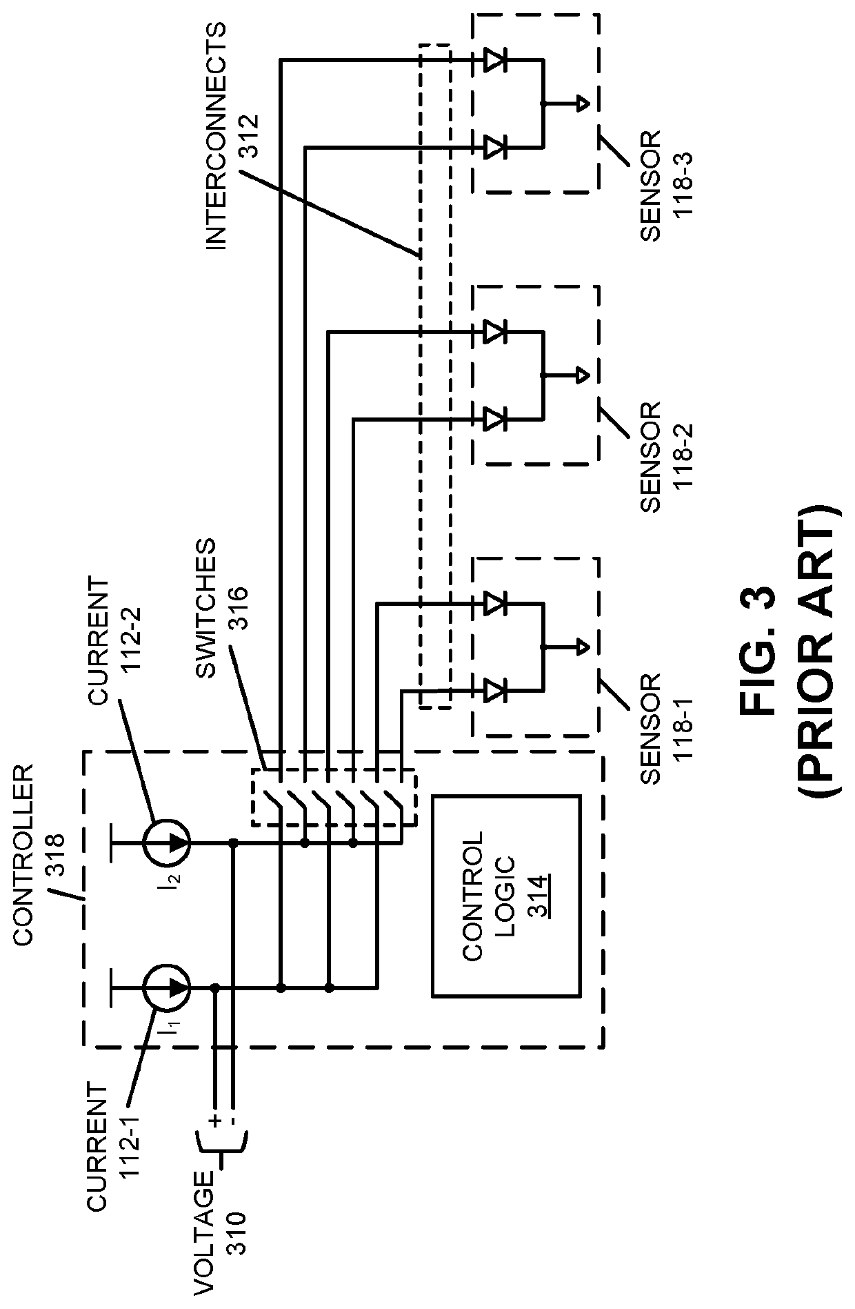
However, because sensitive analog signals can be disturbed by interference from other signals, these interconnects are often routed with shielding by using additional metals around the sensitive analog signals with a low noise signal (such as a ground) to reduce the coupling to other signals.
These requirements may necessitate that these interconnections are routed by a designer (as opposed to using automated design tools), which may make these interconnections more complicated and more expensive.
Additionally, the shielding requirement may use significant metallization resources, particularly in cases where one shielded interconnection must cross another one.
This can cause routing congestion and manual rework further increasing design time and expense.
Alternatively, it may increase the manufacturing cost if additional metal layers are added to the manufacturing process in order to provide an additional metallization resource.
This congestion may particularly problematic in the area near controller 318, because the various shielded analog signal bundles are all routed to this location.
Existing designs also typically lack flexibility, such as the ability to change the number of sensors 118.
Alternatively, if the number of channels is made large enough so that it unlikely that a semiconductor chip will need more sensors 118 than controller 318 can accommodate, then controller 318 may become excessively large, and may include numerous unused analog multiplexer channels.
Furthermore, the number of temperature sensors in the integrated circuit may be limited by a number of bits used for addressing the temperature sensors.

Method used


Image

  • Multi-Sensing PTAT for Multiple-Location Temperature Sensing
  • Multi-Sensing PTAT for Multiple-Location Temperature Sensing
  • Multi-Sensing PTAT for Multiple-Location Temperature Sensing

Examples


Embodiment Construction

[0037]An integrated circuit that controls distributed temperature sensors in a semiconductor die is described. This integrated circuit may include: memory; a controller (such as a PTAT controller) coupled to the memory; temperature sensors distributed at measurement locations in the semiconductor die (such as remote locations from the controller), where a given temperature sensor includes building blocks (or components) that are common to the temperature sensors; and routing between the controller and the building blocks over an addressable bus, where signal lines for analog signals in the addressable bus are reused when communicating between the controller and different temperature sensors.

[0038]By communicating with the temperature sensors over an addressable bus, these measurement techniques may reduce the complexity of designing and fabricating the integrated circuit. For example, the routing in the integrated circuit may be simpler and may avoid crossing of the signal lines. Mo...


PUM

PropertyMeasurementUnit
voltageaaaaaaaaaa
currentaaaaaaaaaa
voltageaaaaaaaaaa

Abstract

An integrated circuit that controls distributed temperature sensors in a semiconductor die is described. This integrated circuit may include: memory; a controller (such as a PTAT controller) coupled to the memory; temperature sensors distributed at measurement locations in the semiconductor die (such as remote locations from the controller), where a given temperature sensor includes building blocks (or components) that are common to the temperature sensors; and routing between the controller and the building blocks over an addressable bus, where signal lines for analog signals in the addressable bus are reused when communicating between the controller and different temperature sensors.

Description

BACKGROUNDField[0001]The present disclosure relates to an integrated circuit that includes semiconductor temperature sensors.Related Art[0002]Integrated circuits often incorporate temperature sensors. These temperature sensors may be used to measure the temperature at some location on the semiconductor die. Moreover, a temperature sensor may be used to monitor over-temperature for components with high power consumption, which may allow remedial action, such as reducing the power consumption when there is danger of overheating. More generally, when a performance characteristic of a component has a temperature dependence, measuring the temperature of a component may allow corrective action to be taken. However, these management techniques depend on accurate measurements of temperature in a semiconductor die. Furthermore, because the management techniques use the local temperature of the component being monitored, multiple components in a semiconductor die may require individual temper...

Claims


Application Information

Patent Timeline
Patent Type & Authority Applications(United States)
IPC IPC(8): G01K7/01G01K13/00
CPCG01K7/01G01K13/00G05D23/1927G05D23/193G05D23/1932G05D23/2034
Inventor KEE, SCOTT DAVID
Owner AYDEEKAY LLC DBA INDIE SEMICON
Learn More