Fabrication of low-cost long wavelength vcsel with optical confinement control

a technology of optical confinement control and fabrication process, which is applied in the direction of semiconductor lasers, electrical equipment, laser details, etc., can solve the problems of sacrificing one inp and one gaas substrate, reducing the production efficiency of dbr layers of semiconductor distributed bragg reflectors, and reducing the production efficiency of dbr layers

Active Publication Date: 2022-06-30
MELLANOX TECHNOLOGIES LTD
View PDF5 Cites 0 Cited by
  • Summary
  • Abstract
  • Description
  • Claims
  • Application Information

AI Technical Summary

Problems solved by technology

Although design and fabrication of reliable short wavelength VCSELs by processing of epitaxial structures grown on gallium arsenide (GaAs) substrates are well developed and accepted by mass production industry, design and fabrication of long wavelength (LW) VCSELs within the wavelength range of 1200-1650 nm have not yet reached the same level of maturity, both from a performance and reliability perspective and from a cost per VCSEL chip point of view.
However, among several disadvantages of wafer fused designs, the most significant ones are: (i) the sacrifice of one InP and one GaAs substrates; (ii) the higher cost of epitaxial growth of semiconductor distributed Bragg reflector DBR layers as compared to DBRs formed of dielectric materials; and (iii) high sensitivity of the bonding process to surface morphology of the epi grown wafers.
The essential difficulty in acquiring acceptable morphology for bonding is at regrowth of InP on patterned TJ, which forms a nonplanar

Method used


Image

  • Fabrication of low-cost long wavelength vcsel with optical confinement control
  • Fabrication of low-cost long wavelength vcsel with optical confinement control
  • Fabrication of low-cost long wavelength vcsel with optical confinement control

Examples


Embodiment Construction

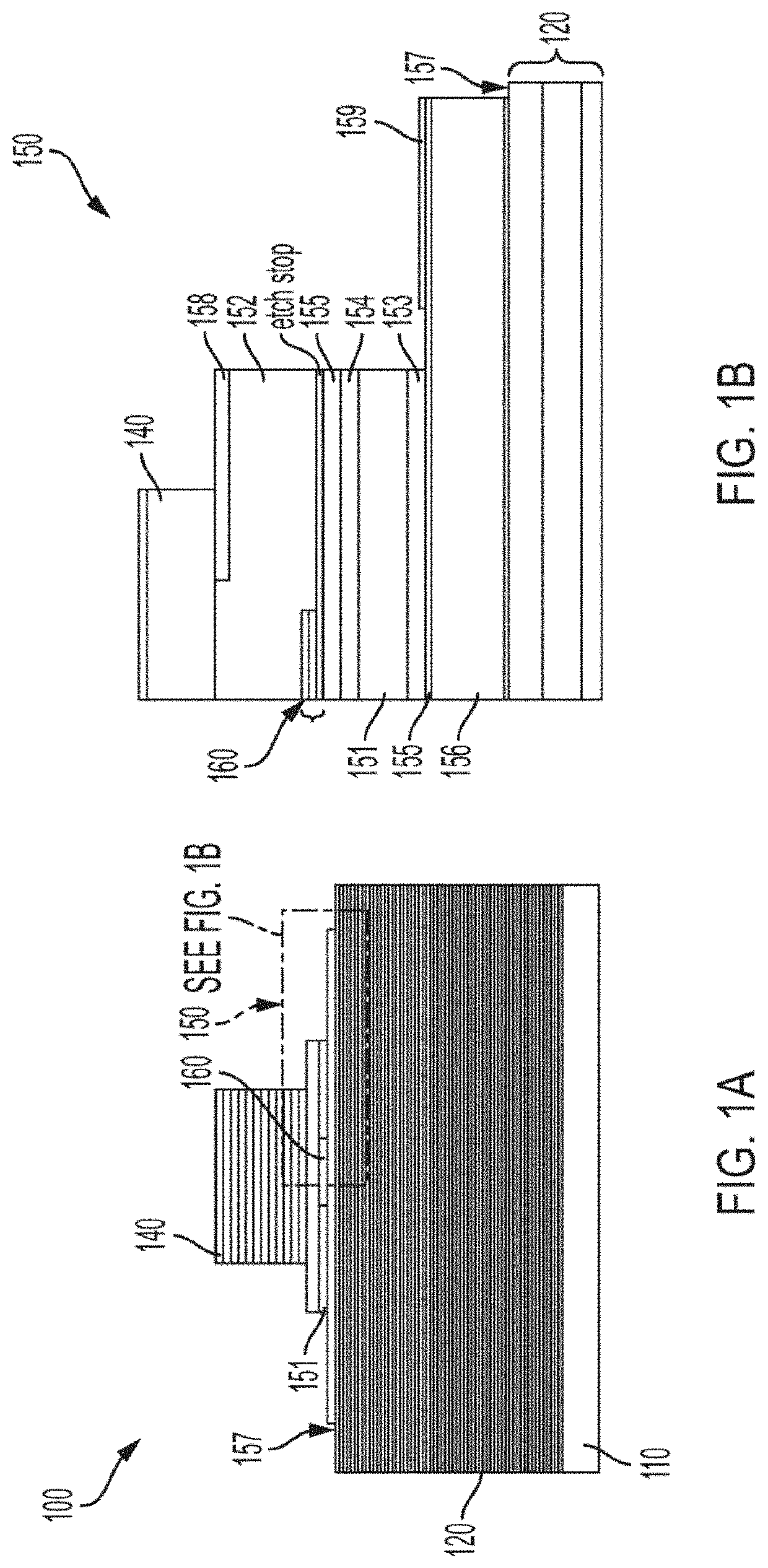
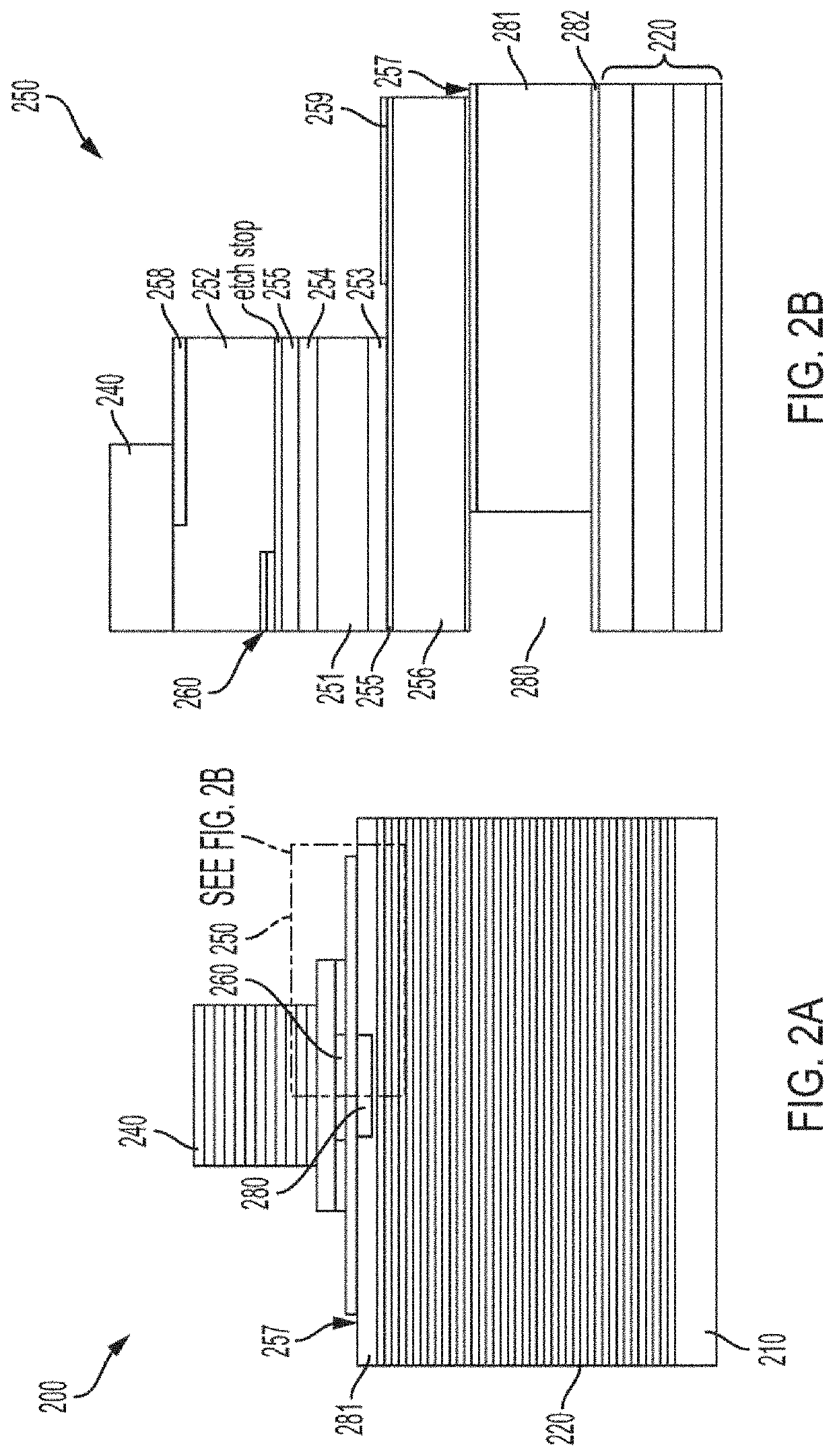
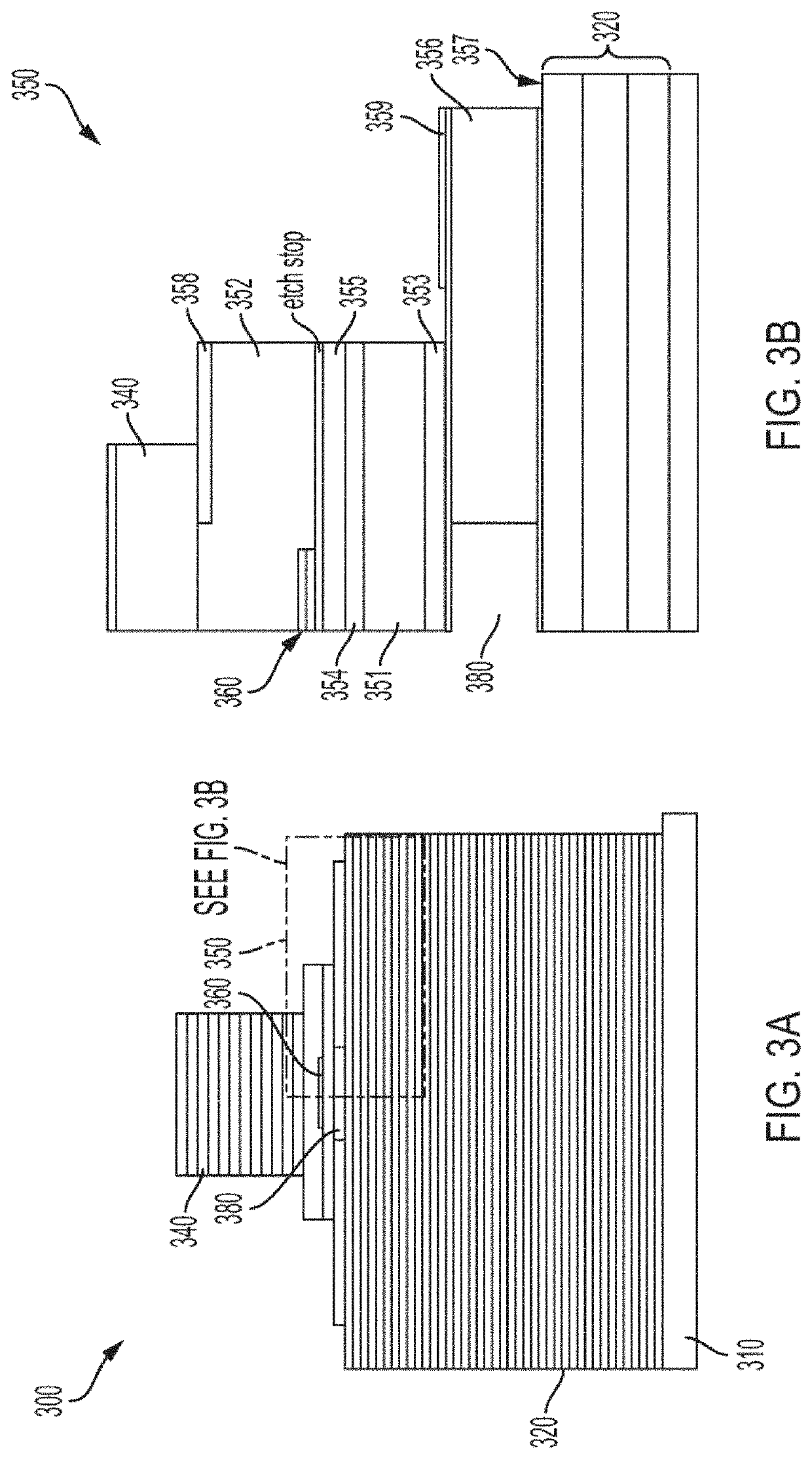
[0045]The present invention now will be described more fully hereinafter with reference to the accompanying drawings, in which some, but not all embodiments of the invention are shown. Indeed, the invention may be embodied in many different forms and should not be construed as limited to the embodiments set forth herein; rather, these embodiments are provided so that this disclosure will satisfy applicable legal requirements. Like numbers refer to like elements throughout.

[0046]In various embodiments, description is made with reference to figures. However, certain embodiments may be practiced without one or more of these specific details, or in combination with other known methods and configurations. In the following description, numerous specific details are set forth, such as specific configurations, dimensions and processes, etc., in order to provide a thorough understanding of the embodiments. In other instances, well-known processes and manufacturing techniques have not been de...


PUM


Abstract

Several VCSEL devices for long wavelength applications in wavelength range of 1200-1600 nm are described. These devices include an active region between a semiconductor DBR on a GaAs wafer and a dielectric DBR regrown on the active region. The active region includes multi-quantum layers (MQLs) confined between the active n-InP and p-InAlAs layers and a tunnel junction layer above the MQLs. The semiconductor DBR is fused to the bottom of the active region by a wafer bonding process. The design simplifies integrating the reflectors and the active region stack by having only one wafer bonding followed by regrowth of the other layers including the dielectric DBR. An air gap is fabricated either in an n-InP layer of the active region or in an air gap spacer layer on top of the semiconductor DBR. The air gap enhances optical confinement of the VCSEL. The air gap may also contain a grating.

Description

TECHNICAL FIELD[0001]Embodiments described herein relate to lasers for fiber-optic data and analog transmission, and more particularly, for design and fabrication of long wavelength VCSELs with optical confinement.BACKGROUND[0002]The use of vertical-cavity surface-emitting lasers (VCSELs) for optical transmission in fiber optic systems has provided several advantages over commonly used edge-emitting lasers. For example, VCSELs require less power consumption and can be manufactured more efficiently than edge-emitting lasers. One aspect of this efficiency is provided by the on-wafer testing capability of VCSELs. The ability to conduct on-wafer testing results in a considerable cost advantage compared with conventional testing techniques used for edge emitting lasers. Furthermore, VCSELs provide reliable operation over time, which is essential for applications in fiber optic systems.[0003]Although design and fabrication of reliable short wavelength VCSELs by processing of epitaxial str...

Claims


Application Information

Patent Timeline
IPC IPC(8): H01S5/183H01S5/30H01S5/343H01S5/125H01S5/20H01S5/042
CPCH01S5/18316H01S5/18369H01S5/18377H01S5/1838H01S5/04252H01S5/34306H01S5/125H01S5/209H01S5/3095H01S5/18361H01S5/18308H01S5/04257H01S5/18319H01S5/18327
Inventor BERK, YURILAKOVLEV, VLADIMIRSHARKAZ, TAMIRMENTOVICH, ELADGALANTY, MATANKALIFA, LTSHAK
Owner MELLANOX TECHNOLOGIES LTD
Why Eureka
Try Eureka