

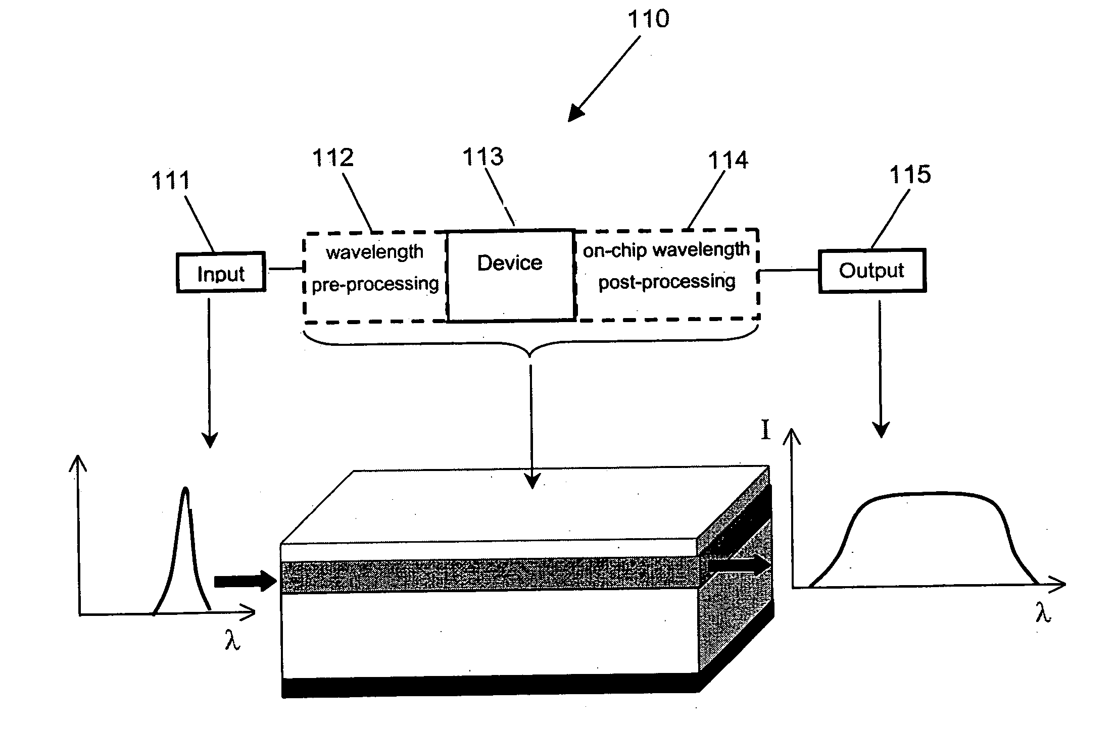
Nonlinear optical device
a technology of optical devices and optical components, applied in the direction of optical elements, instruments, optical waveguide light guides, etc., can solve the problems of reducing the energy damage threshold, high attendant risk of surface or bulk damage to the sample, and generating other wavelengths using nonlinear optical processes, etc., to achieve efficient nonlinear interaction, enhance bandwidth access, and high intensity
- Summary
- Abstract
- Description
- Claims
- Application Information
AI Technical Summary
Benefits of technology
Problems solved by technology
Method used
Image

Examples
embodiment 210
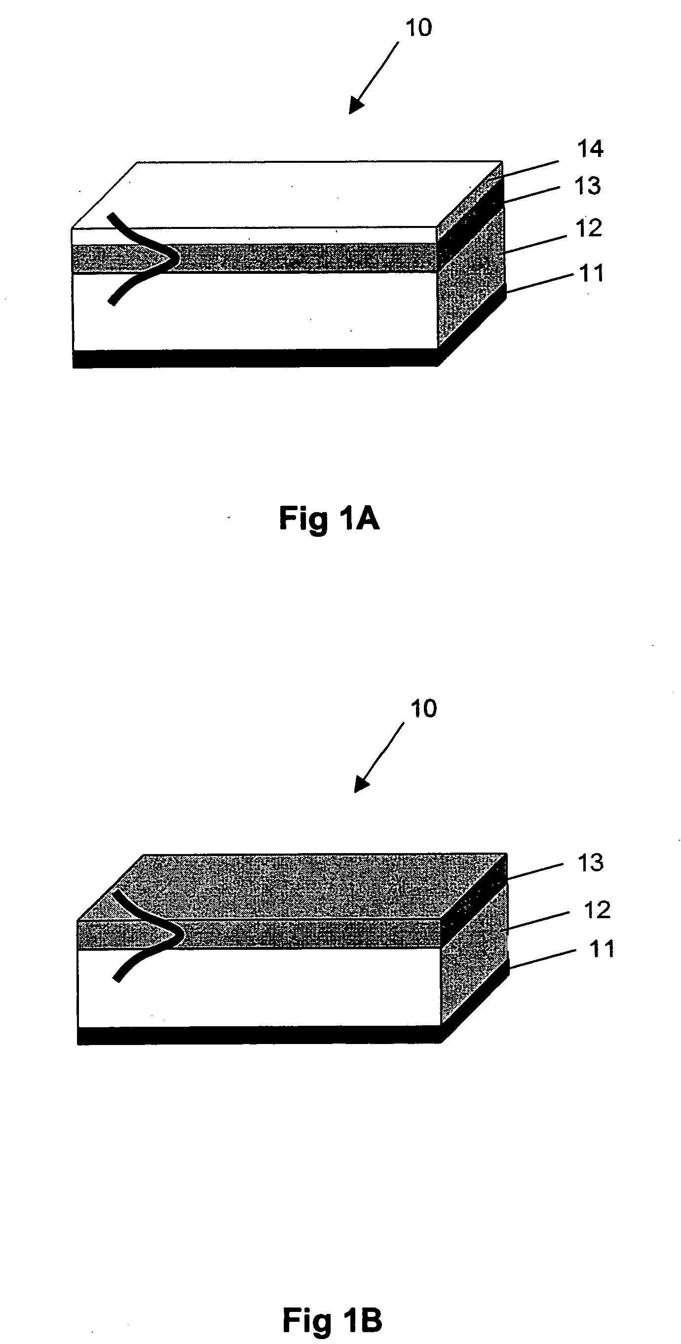
FIG. 21 illustrates a ridge embodiment 210 having a horizontally tapered input region 214 for spot size conversion and improved optical coupling efficiency. A vertical taper may also be employed. The structure 210 includes a buffer layer 212 and a core layer 213. On the core layer 213 is a core ridge layer 215 and it is the ridge layer that is tapered at input region 214.
FIG. 22 illustrates the same design applied to a rib structure 220. The structure includes a buffer layer 222 and a core rib layer 224. An input region 223 of the rib layer 224 is horizontally tapered for spot size conversion and improved optical coupling efficiency. A vertical taper may also be employed.
In a manner analogous to FIG. 16, FIG. 23 illustrates the combination of tapers and photonic crystal structures applied to a ridge waveguide embodiment of th present invention. FIG. 23 shows a device 230 including a buffer layer 232, a core layer 233 and a core ridge layer. The core ridge layer includes a tapered ...
embodiment 280
Furthermore, operating near the zero dispersion point can lead to broader continuum generation. FIG. 28 illustrates an example of this embodiment 280 having a 2-D photonic crystal structure 284 that extends from the cladding layer 285, through the core layer 283 and into the buffer layer 282. The 2-D structure permits additional functionality such as beam shaping within the generating region.
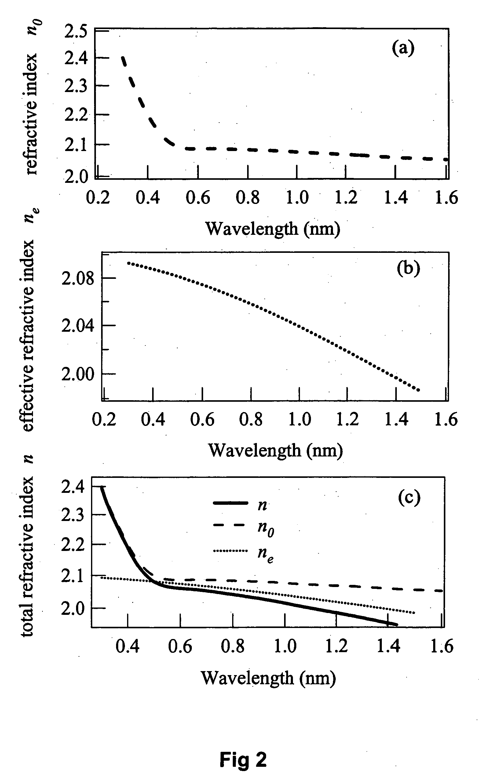
An alternative device structure for modifying the dispersion characteristics of the waveguide is a multilayered structure 290, as illustrated in FIG. 29. Here, the “core”296 comprises alternating layers 293, 294, 295 of high (n1, n2 . . . nn) refractive index and low refractive index on a buffer layer 292. The dimensions and materials used for each layer are calculated according to the desired dispersion characteristics. In this manner three different spectral outputs can be obtained from a single input.
As has been described previously, in relation to tapers, the planar waveguide device may c...
embodiment 370
FIG. 37 shows another embodiment 370 comprising an extended waveguide 372 with input 371 and output 374 tapers, and on-chip beam splitters 373 to couple light out into the feedback loop. Wavelength selectivity and tuning is provided by photonic crystal 375 located within the feedback loop.
Optical parametric amplification of a second input beam at the signal or idler wavelength is also possible using a planar waveguide according to the present invention. The arrangement is much the same as the OPO above but without any feedback mechanism. In all parametric device embodiments it is preferred that the nonlinearly generating region comprises a structure to modify the dispersion of th planar waveguide. This may be provided by photonic crystal structures or multilayer structures as described above, or any other suitable structure. In order for accurate phase-matching and efficient operation to be achieved, it is preferred that the total dispersion is in the anomalous regime for the wavel...
PUM
| Property | Measurement | Unit |
|---|---|---|
| refractive index | aaaaa | aaaaa |
| thick | aaaaa | aaaaa |
| thick | aaaaa | aaaaa |
Abstract
Description
Claims
Application Information