P-type semiconductor zinc oxide films process for preparation thereof, and pulsed laser deposition method using transparent substrates

a technology of zinc oxide films and semiconductors, applied in the field of p-type semiconductor zinc oxide films, can solve the problems of large number of native donor defects to overcome, unstable mono-doped zno with group-v elements, and large number of native donor defects to achieve the effect of high carrier concentration and high conductivity

Inactive Publication Date: 2007-10-18
IMRA AMERICA
View PDF9 Cites 35 Cited by
  • Summary
  • Abstract
  • Description
  • Claims
  • Application Information

AI Technical Summary

Benefits of technology

[0015] One object of this invention is to provide a simple and reproducible process to fabricate p-type ZnO film with high carrier concentration and high conductivity. This method uses two dopant elements to achieve this object.
[0019] This invention uses a femtosecond or similar ultrashort pulse laser as the energy source for ablation. Compared with nanosecond laser pulses, femtosecond to picosecond laser pulses have much higher peak power due to their ultrashort pulse duration, and the ablation mechanism is also intrinsically different from that of nanosecond laser ablation. One fundamental difference is that within the femtosecond pulse duration, heat conduction in the target material is negligible, and therefore the ablation basically occurs in a non-melting regime. (D. Linde, et al, Applied Surface Science, 109 / 110, 1, 1997; E. G. Gamaly, et al, Applied Surface Science, 197-8, 699, 2002; Z. Zhang, et al, Journal of Applied Physics, 92-5, 2867, 2002). Consequently in femtosecond PLD, droplet free growth of thin films can be obtained.
[0020] To incorporate different dopant elements into the film, this invention uses a solid target made of ZnO powders mixed with different impurity compounds. Using such a mixed solid target largely simplifies the doping process in growth. For example, one can simply choose compounds that contain the desired dopant elements. And the dopant concentration can be controlled by varying the weight percentage of the impurity compound. In particular, one of the novel aspects of this invention regarding making the target is to mix ZnO powders with lithium phosphate (Li3PO4) powders which naturally contain both Li and P dopants. Compared with other methods of doping that use gas sources (for example precursors in CVD) and evaporation sources, this method is easy and cost-effective to perform, and generates negligible negative environmental effect.

Problems solved by technology

On the other hand, ZnO is naturally an n-type material, which means that there is a large number of native donor defects to overcome in order to make it p-type.
In practice, mono-doping ZnO with Li only results in semi-insulating ZnO, which is due to self-compensation of Li-related donor defects; and mono-doped ZnO with group-V elements is often unstable, mostly due to the low solubility of those elements and dopant-induced donor defects.
This has impeded the wide application of nanosecond PLD in industrial production.

Method used


Image

  • P-type semiconductor zinc oxide films process for preparation thereof, and pulsed laser deposition method using transparent substrates
  • P-type semiconductor zinc oxide films process for preparation thereof, and pulsed laser deposition method using transparent substrates
  • P-type semiconductor zinc oxide films process for preparation thereof, and pulsed laser deposition method using transparent substrates

Examples


Embodiment Construction

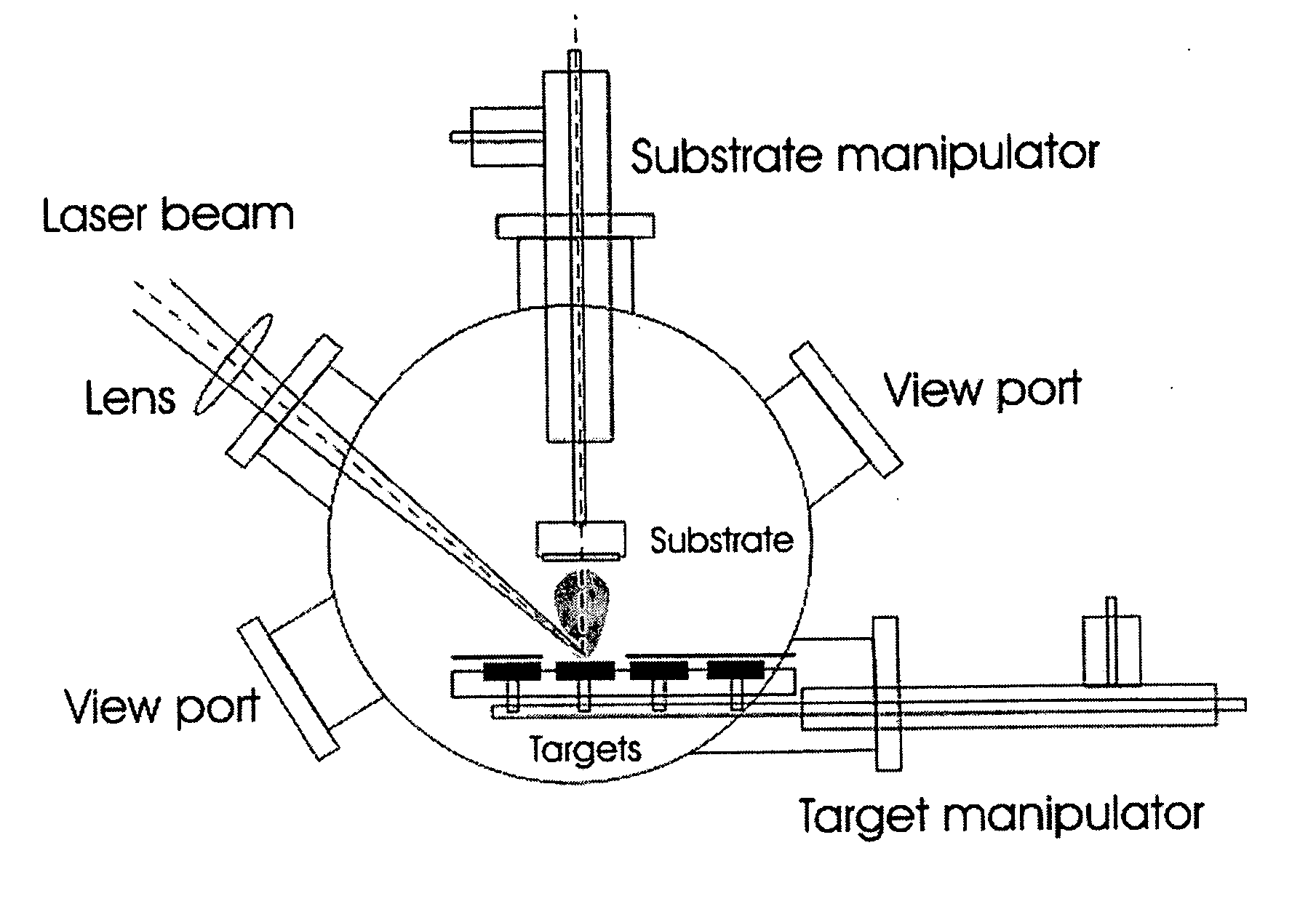
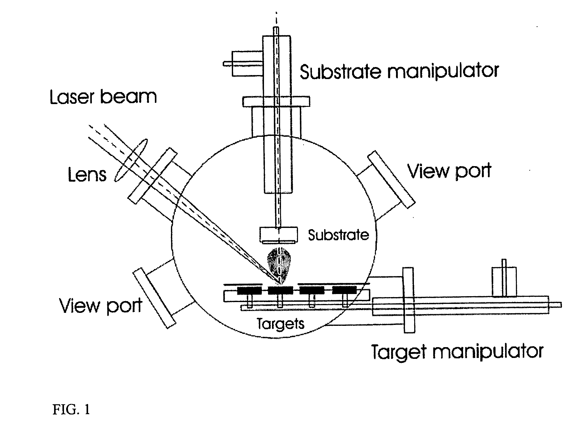
[0034] The present invention first provides an economic and reliable method for fabricating p-type semiconductor ZnO films. The fabrication procedure includes making of the ablation target, vacuum laser ablation of the target and thin film deposition, and post-growth annealing. The setup of a femtosecond pulsed laser deposition (fs-PLD) system is schematically shown in FIG. 1.

[0035] The target for laser ablation is made of a mixture of ZnO powders with lithium phosphate (Li3PO4) powders of up to 2 wt %. Using lithium phosphate is an efficient way of simultaneous introduction of the two dopants. The mixed powders are first compressed with a hydraulic compressor with a pressure of 2-6 ton / cm2. The solid target disk is then sintered for 10 hrs at temperatures up to 1000° C. During sintering, the target is buried in ZnO powders to avoid decomposition. The target thus made has a density of 90%. A high density (at least 80%) target is preferred for reducing particles in the ablation plum...


PUM

PropertyMeasurementUnit
temperatureaaaaaaaaaa
distanceaaaaaaaaaa
temperaturesaaaaaaaaaa

Abstract

A p-type semiconductor zinc oxide (ZnO) film and a process for preparing the film are disclosed. The film is co-doped with phosphorous (P) and lithium (Li). A pulsed laser deposition scheme is described for use in growing the film. Further described is a process of pulsed laser deposition using transparent substrates which includes a pulsed laser source, a substrate that is transparent at the wavelength of the pulsed laser, and a multi-target system. The optical path of the pulsed laser is arranged in such a way that the pulsed laser is incident from the back of the substrate, passes through the substrate, and then focuses on the target. By translating the substrate towards the target, this geometric arrangement enables deposition of small features utilizing the root of the ablation plume, which can exist in a one-dimensional transition stage along the target surface normal, before the angular width of the plume is broadened by three-dimensional adiabatic expansion. This can provide small deposition feature sizes, which can be similar in size to the laser focal spot, and provides a novel method for direct deposition of patterned materials.

Description

BACKGROUND [0001] 1. Field of the Invention [0002] This invention relates to the fabrication of semiconductor ZnO (zinc oxide) for application in electric and optoelectric devices. Particularly, this invention provides a simple and reproducible process to dope ZnO to make this material have a p-type conductivity. This invention is also related to the process of pulsed laser deposition of transparent thin films, particularly to the deposition of large area transparent thin films and multilayer periodic dielectric structures on transparent substrates. [0003] 2. Description of the Related Art [0004] ZnO is a semiconductor material with a large direct band-gap of 3.37 eV at room temperature. Due to this large band-gap and a large exciton binding energy (60 meV), ZnO has great potential for use in short-wavelength optoelectronic devices, such as light-emitting diodes (LEDs), laser diodes (LDs), and ultraviolet light detectors. In the past years, this field has been dominated by other mat...

Claims


Application Information

Patent Timeline
Patent Type & Authority Applications(United States)
IPC IPC(8): C23C16/00C23C14/30
CPCC23C14/083C23C14/22C23C14/28C23C14/34
Inventor LIU, BINGHU, ZHENDONGCHE, YONGUEHARA, YUZURU
Owner IMRA AMERICA
Why Eureka
Try Eureka