Nonlinear optical device

a technology of optical devices and optical waveguides, applied in the direction of optics, optical waveguide light guides, instruments, etc., can solve the problems of reducing the energy damage threshold, high attendant risk of surface or bulk damage to the sample, and generating other wavelengths using nonlinear optical processes, etc., to achieve efficient nonlinear interaction, enhance bandwidth access, and high intensity

Inactive Publication Date: 2005-03-03
MESOPHOTONICS LTD
View PDF3 Cites 48 Cited by
  • Summary
  • Abstract
  • Description
  • Claims
  • Application Information

AI Technical Summary

Benefits of technology

In addition to the simple broad area broad area waveguide configuration, a nonlinear device according to the present invention may comprise other forms of planar waveguide structure, which may provide enhanced optical confinement. Preferably, the planar waveguide comprises a ridge waveguide. Alternatively, the planar waveguide may comprise a rib waveguide.
One of the problems associated with planar structures, is the coupling in of light from other devices or sources having a different geometry, such as optical fibre. This problem can be mitigated by employing beam shaping or spot-size converting structures, which can be integrated on the same chip.
Preferably, the non-linear optical device has a structure which is operative to compress temporally the optical input and / or optical output. Pulse compression can serve to increase pulse peak power, leading to a stronger induced nonlinear effect, and can also pre-compensate for pulse broadening during subsequent propagation due to refractive index dispersion.
Preferably, the non-linear optical device has a structure which is operative to modify the optical dispersion characteristics of the planar optical waveguide. The structure will typically be disposed either proximate or in the region of nonlinear signal generation, and can serve to tailor the waveguide dispersion characteristics to optimize device performance and accessible bandwidth enhancement.
Preferably, the interferometer comprises a photonic integrated circuit, allowing easy integration of all the components on a single chip.
Thus the present invention provides an extremely flexible nonlinear device, which substantially enhances the bandwidth accessible in a nonlinear optical interaction. The key element of the device is a planar waveguide formed from material having both high linear and nonlinear refractive index, which combines the advantages of strong optical confinement and high intensity over an extended interaction region with those of a highly nonlinear material. The net result is an extremely efficient nonlinear interaction with a considerably enhanced accessible bandwidth, as compared to that achievable in prior art planar devices. The device has particular application in optical continuum and supercontinuum generation and also in broadly tunable parametric devices. The geometry of the planar device makes it particularly amenable to the integration of other functionality on the same chip and also compatible with modern photonic integrated circuits. By using tapers, ridge and rib waveguides, and also pulse compression, dispersion modifying and filtering structures (particularly photonic crystal structures) the performance and range of applications of the device can be greatly improved. The planar waveguide device may be incorporated in more complex photonic integrated circuits, such as a Michelson interferometer for low coherence interferometry based optical coherence tomography.

Problems solved by technology

However, as many laser sources only operate over narrower, well-defined wavelength ranges, nonlinear optical processes have been employed to generate other wavelengths using the output from available laser sources.
However, as will now be described, all of these have their attendant drawbacks.
However, due the low nonlinear coefficient associated with many materials, the characteristic threshold intensity is high and so a high peak intensity laser source is required.
Consequently, there is a high attendant risk of surface or bulk damage to the sample unless it is a material exhibiting a high damage threshold such as sapphire, which also exhibits good stability of CG.
Nevertheless, the associated pulse energy damage threshold is also reduced and so end facet damage may occur, requiring the cleaving of a new facet or provision of a new fiber entirely.
In addition, the stability of CG in optical fibers is typically low, the overall size may limit the compactness of the source and the optical mode properties are not easily compatible with the planar waveguide devices used in photonic integrated circuits.
A further problem is maintaining the polarization (electric field orientation) of the light generated, which affects its usefulness in applications.
Another issue associated with CG is the characteristic optical dispersion (variation of refractive index with wavelength) of the device in which the continuum is generated.
But for waveguides, the situation is more complex, with the total dispersion also depending on waveguide and modal dispersion.
However, despite the improvement in CG bandwidth, the microstructured fibers still suffer from the drawbacks associated with more conventional fibers, as outlined above.
In addition, there are many materials that can not be fabricated in bulk or fiber form and are therefore unavailable for CG in these configurations.
However, although the process was accompanied by nonlinear spectral broadening, which resulted in an optical output having a bandwidth broader than that of the input pulse, the degree of spectral broadening was not sufficient to generate an optical continuum.
Although improved performance is obtained in terms of threshold power and conversion efficiency, the available tuning range is still limited.

Method used


Image

  • Nonlinear optical device
  • Nonlinear optical device
  • Nonlinear optical device

Examples


embodiment 130

FIG. 13 shows an embodiment 130 with two adjacent horizontally (laterally) tapering input regions 131 prior to the main interaction region 132. This embodiment allows for the independent coupling of two separate beams into the waveguide or, alternatively, a more complex coupling of a single large beam into the waveguide. Again, the input beam 133 reduces in size 134 as it propagates. With a slow smooth taper, input light is adiabatically coupled into a mode supported by the waveguide and able to propagate therein. Provision of an on-chip spot-size converter increases the range of light delivery systems that can be used with the waveguide device, including optical fiber.

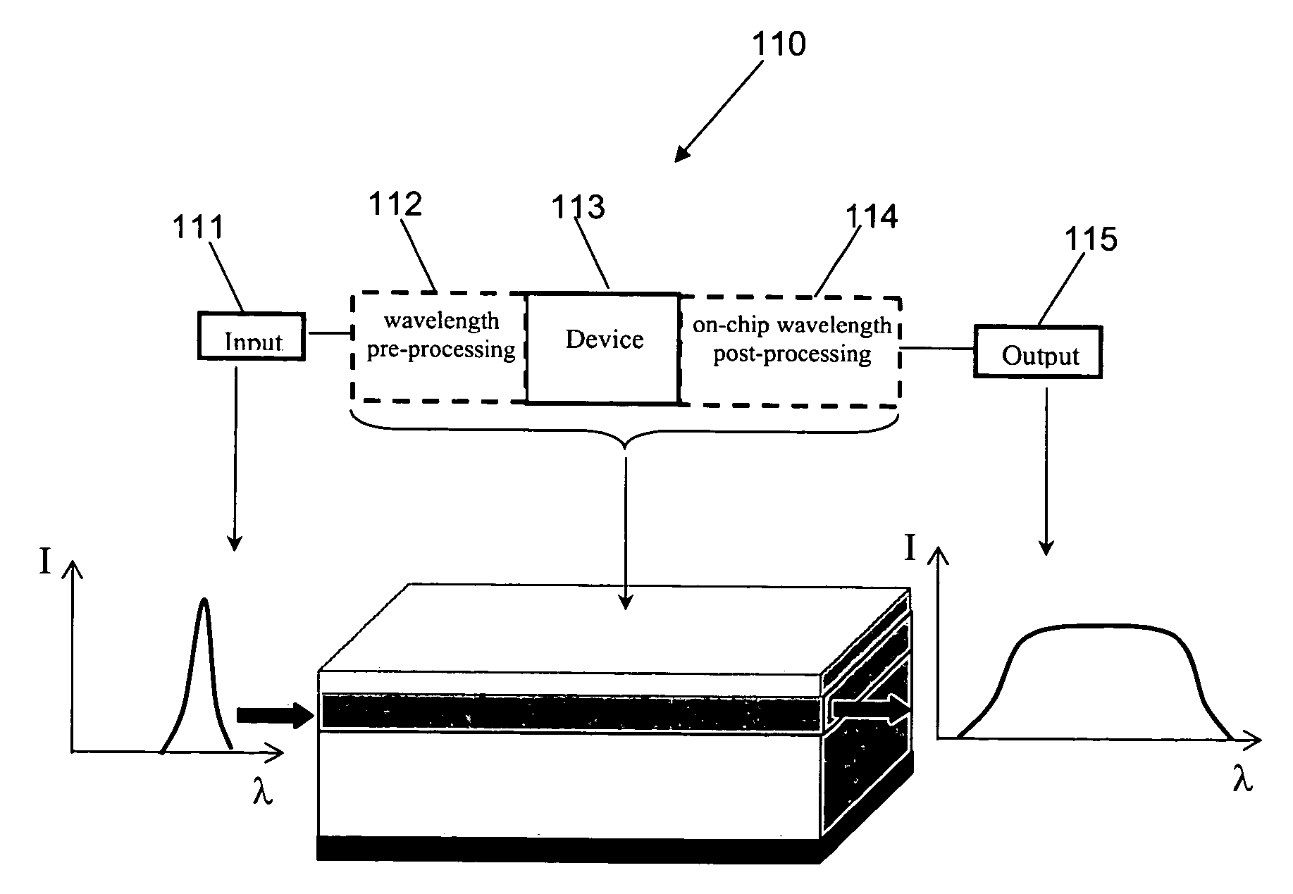
Adding on-chip functionality is one of the great advantages of planar waveguide devices. On-chip structures for spatial profiling and beam shaping have already been described in the context of waveguide tapers. However, other types of functionality can be included that modify the phase or amplitude of a beam propagat...

embodiment 210

FIG. 21 illustrates a ridge embodiment 210 having a horizontally tapered input region 214 for spot size conversion and improved optical coupling efficiency. A vertical taper may also be employed. The structure 210 includes a buffer layer 212 and a core layer 213. On the core layer 213 is a core ridge layer 215 and it is the ridge layer that is tapered at the input region 214. FIG. 22 illustrates the same design applied to a rib structure 220. The structure includes a buffer layer 222 and a core rib layer 224. An input region 223 of the rib layer 224 is horizontally tapered for spot size conversion and improved optical coupling efficiency. A vertical taper may also be employed.

FIG. 23 illustrates other types of taper structure that may be implemented in a ridge (or rib) waveguide. Again the basic structure 230 comprises a buffer layer 231, a core layer 232 and a core ridge layer 233. Both of the two core ridges shown provide lateral confinement and have input waveguide regions 234 wi...

embodiment 280

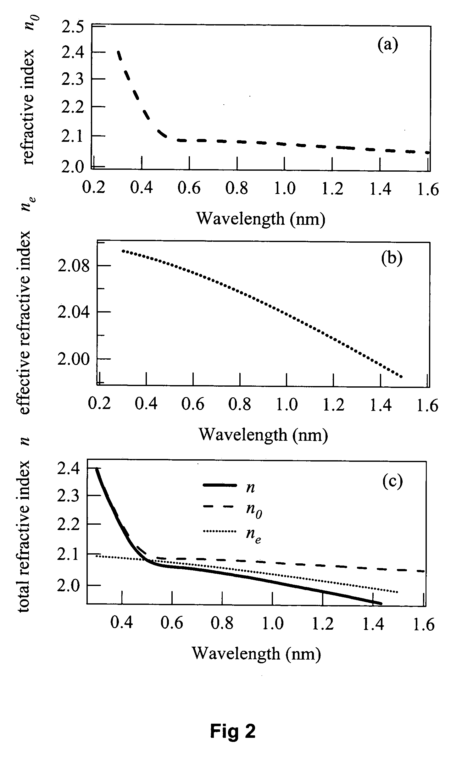
Furthermore, operating near the zero dispersion point can lead to broader continuum generation. FIG. 28 illustrates an example of this embodiment 280 having a 2-D photonic crystal structure 284 that extends from the cladding layer 285, through the core layer 283 and into the buffer layer 282. The 2-D structure permits additional functionality such as beam shaping within the generating region.

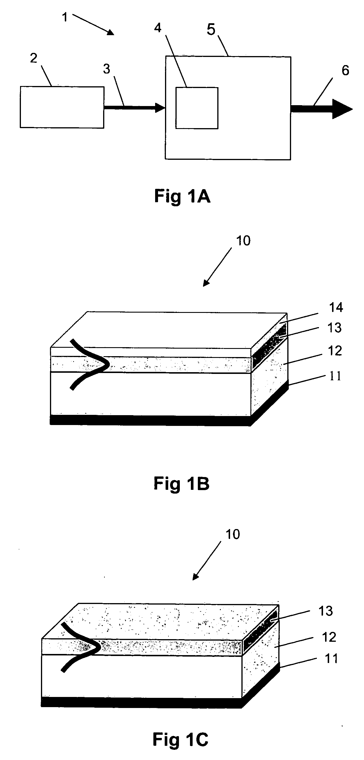
An alternative device structure for modifying the dispersion characteristics of the waveguide is a multilayered structure 290, as illustrated in FIG. 29. Here, the “core”296 comprises alternating layers 293, 294, 295 of high and low refractive index (n1, n2 . . . nn) on a buffer layer 292. The dimensions and materials used for each layer are calculated according to the desired dispersion characteristics. In this manner, as shown, three different spectral outputs can be obtained from a single input.

As has been described previously, in relation to tapers, the planar waveguide device may compris...


PUM

PropertyMeasurementUnit
refractive indexaaaaaaaaaa
thickaaaaaaaaaa
thickaaaaaaaaaa

Abstract

There is provided a non-linear optical device for enhancing the bandwidth accessible in the nonlinear generation of an optical signal. The device comprises a planar optical waveguide, the planar optical waveguide being operative to generate an optical output from an optical input having an input bandwidth by means of a non-linear optical process, the optical output having a wavelength within an accessible bandwidth, wherein the planar optical waveguide is operative to enhance the accessible bandwidth such that the ratio of the accessible bandwidth to the input bandwidth is at least 4. The device is particularly applicable to broad optical continuum generation, but may also be used in a parametric oscillator or amplifier arrangement with broad tuning range. The planar waveguide geometry permits easy integration in more complex photonic integrated circuits such as a Michelson interferometer for low coherence interferometry based optical coherence tomography.

Description

FIELD OF THE INVENTION The present invention relates to nonlinear optical devices and in particular to a planar waveguide device for nonlinear optical signal generation with large accessible bandwidth, including optical continuum generation. BACKGROUND TO THE INVENTION Optical sources which can generate radiation over a wide wavelength range currently have many applications in scientific research, engineering and medicine. Often the application requires the coherence properties associated with laser radiation and so various laser materials have been developed which exhibit a broad gain bandwidth when suitably pumped. A good example is titanium doped sapphire, which is characterized by a gain bandwidth covering the range 650-1100 nm. The coherence properties of lasers based on broadband material systems may be further enhanced in a number of ways. The technique of modelocking permits the utilization of much of the available laser bandwidth to obtain a repetitive train of short (or ...

Claims


Application Information

Patent Timeline
Patent Type & Authority Applications(United States)
IPC IPC(8): G02F1/35G02F1/365
CPCG02F1/353G02F2001/3528G02F1/365G02F1/3528
Inventor PARKER, GREGBAUMBERG, JEREMYWILKINSON, JAMESCHARLTON, MARTINZOOROB, MAJDNETTI, MARIA CATERINAPERNEY, NICOLASLINCOLN, JOHN
Owner MESOPHOTONICS LTD
Why Eureka
Try Eureka