
MEMS switch including an embedded metal contact

a technology of metal contacts and switches, applied in the field of relays, can solve the problems of bending of substrates, affecting the operation of switches, etc., and achieve the effect of reliable switching and operation

Pending Publication Date: 2022-10-13
ROBERT BOSCH GMBH
View PDF11 Cites 0 Cited by
  • Summary
  • Abstract
  • Description
  • Claims
  • Application Information

AI Technical Summary

Benefits of technology

This patent is for a new type of MEMS relay that can switch on and off even when there is a current flow through it. One important feature is that the relay uses a negative image of the metal pluggage in silicon to create very narrow gaps between the pluggage. This process allows for very small gap widths, resulting in a self-adjusting process. The patent also explains how trenches filled with tungsten are introduced into a silicon layer, and how a portion of the tungsten surface is exposed via a silicon trenching process. This process creates a deflectable switching element that can activate the relay. Additionally, the patent discusses how the process reduces costs and minimizes tension in the silicon layer. Overall, this patent provides a way to create a reliable and efficient MEMS relay with precise control over gap widths.

Problems solved by technology

If a relay is switched on or off under current, electrical flashovers result which impair the contact surfaces.
A disadvantage of tungsten is that it is a very expensive material that is mechanically difficult to process, for which reason tungsten contacts are used in particular only for this application in relays.
A restriction of this method is that thick metal layers always require a metal deposition in at least the target thickness of the metal plug.
This is particularly critical for tungsten layers, since they may cause stress with regard to the substrate during the deposition, resulting in bending of the substrate.
A further restriction is that, in particular for tungsten and many other metals, on the one hand there are no etching processes that provide very vertical etching flanks in order to achieve large contact areas upon a lateral deflection of the switching portion of the relay.
On the other hand, there are also no etching processes for tungsten and many other metals that are able to create very narrow, deep trenches in order to achieve small distances upon a lateral movement of the contact areas.
In addition to the typical restriction of the known metal etching processes with regard to the shape and the depth of the etching trenches, these etching processes also have poor selectivity toward the resist mask.
This means that one must either use a thick resist mask with poor resolution, i.e., which allows only wide trenches, or a thin resist mask with high resolution is used, but with which only trenches of low depth may be created in tungsten (W).
A further restriction is that according to the conventional structuring of very thick metal layers, a high topography is present on the substrate, and it is technically very difficult or impossible to deposit and structure further layers.
It is often difficult to carry out CVD depositions in narrow trenches.

Method used


Image

  • MEMS switch including an embedded metal contact
  • MEMS switch including an embedded metal contact
  • MEMS switch including an embedded metal contact

Examples


Embodiment Construction

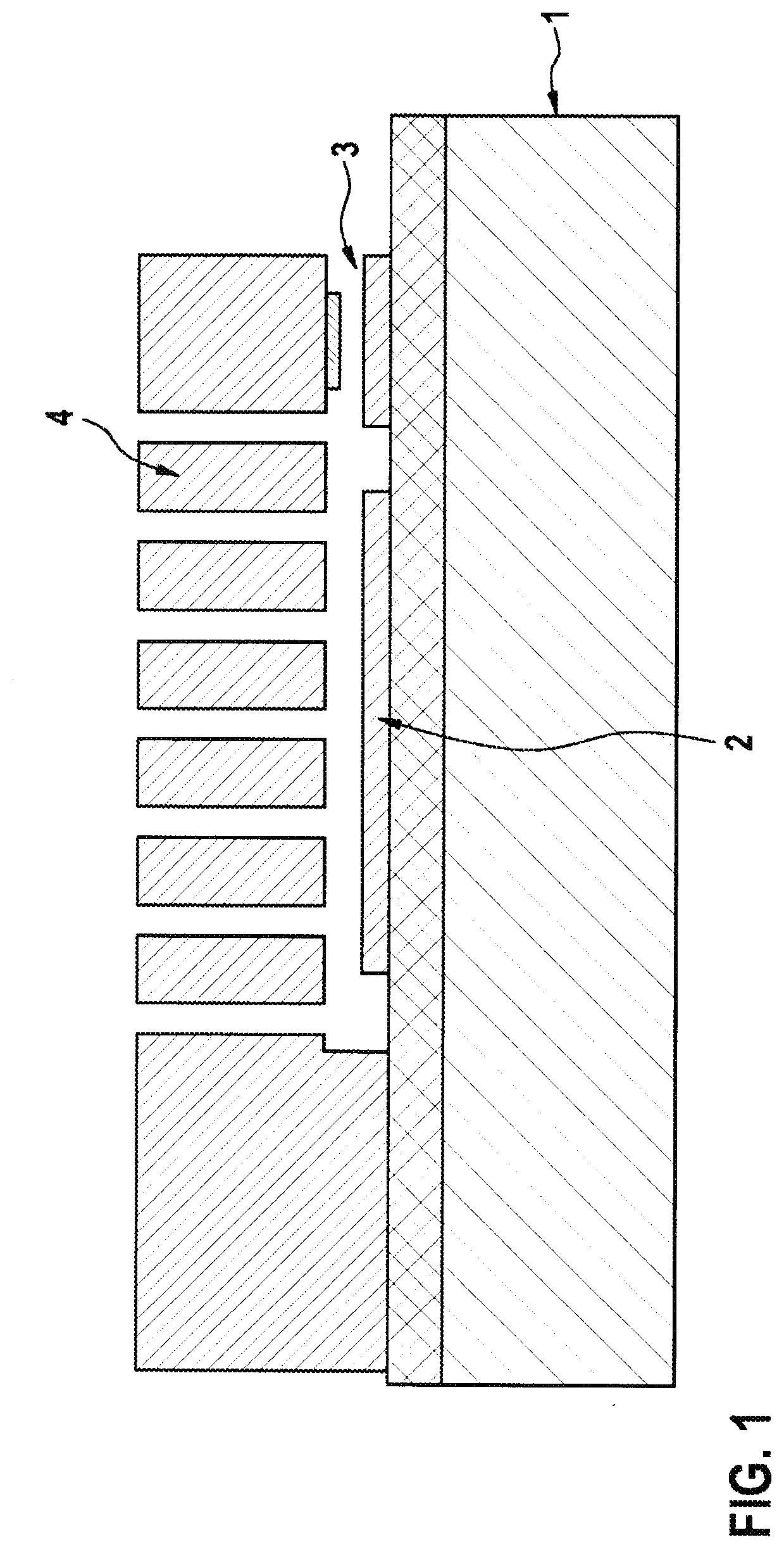
[0031]FIG. 1 schematically shows a capacitively actuatable MEMS switch including an out-of-plane switching element in the related art, in a sectional illustration. A first electrode 2 and a first contact surface 3 are provided on a substrate 1. A lever structure 4 is situated above both structures, separated by a distance. If a voltage is applied between the lever and the first electrode, a movement out of the substrate plane (out-of-plane) results. The lever is deflected essentially perpendicularly toward the substrate, and a contact between the lever and the contact surface is established.

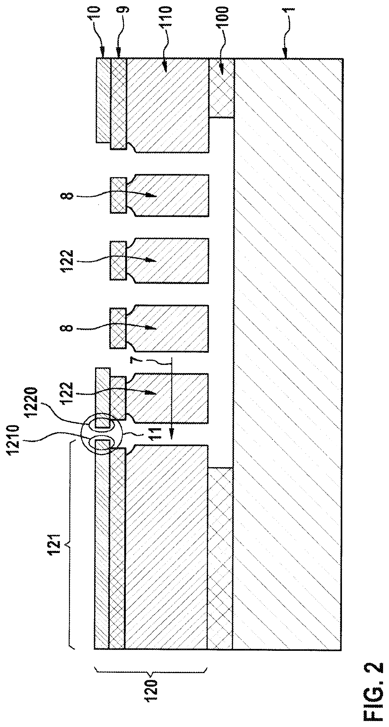
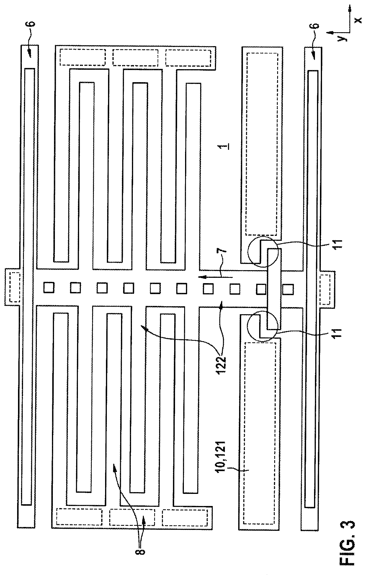
[0032]FIG. 2 schematically shows a capacitively actuatable MEMS switch including an in-plane switching element, in a sectional illustration. A first insulating layer 100, a silicon layer 110, a second insulating layer 9, and a metal layer 10 are situated one on top of the other on a substrate 1. The silicon layer, the second insulating layer, and the metal layer together form a micromechanical fu...


PUM


Abstract

A MEMS switch that includes a substrate with a first insulating layer and a silicon layer thereabove, a fixed portion and a movable switching portion being formed in the silicon layer.A first metal layer is situated in recesses in the silicon layer at a side of the silicon layer facing away from the substrate, the first metal layer forming at least one switchable electrical contact between the fixed portion and the switching portion.A method for manufacturing a MEMS switch including at least one embedded metal contact is also described.

Description

FIELD[0001]The present invention is directed to a MEMS switch that includes a substrate with a first insulating layer and a silicon layer thereabove, a fixed portion and a movable switching portion being formed in the silicon layer.BACKGROUND INFORMATION[0002]There are many different types of relays. Typical miniature relays have a size of approximately 1 cm, are driven via a solenoid, have a certain non-negligible current consumption in the switched-on state, and are optimized for various applications.[0003]To guarantee a long service life and also to enable switching of currents during the switching operation, there are special relays whose contacts are made of tungsten. If a relay is switched on or off under current, electrical flashovers result which impair the contact surfaces. Tungsten is a material that is very robust against flashovers, and therefore guarantees a long service life for this application. A disadvantage of tungsten is that it is a very expensive material that i...

Claims


Application Information

Patent Timeline
IPC IPC(8): H01H1/00H01H11/00
CPCH01H1/0036H01H11/00H01H2001/0057H01H11/06H01L21/32051H01L21/76224H01H2001/0078H01H1/06H01H59/0009
Inventor REINMUTH, JOCHENLEWIS, MATTHEWSCHMOLLNGRUBER, PETER
Owner ROBERT BOSCH GMBH
Learn More