
Manufacturing method for conductive substrate and conductive substrate
a technology of conductive substrate and manufacturing method, which is applied in the direction of conductive layers on insulating supports, instruments, plastic/resin/waxes insulators, etc., can solve the problems that the above characteristics are difficult to be compatible with each other
- Summary
- Abstract
- Description
- Claims
- Application Information
AI Technical Summary
Benefits of technology
Problems solved by technology
Method used
Image

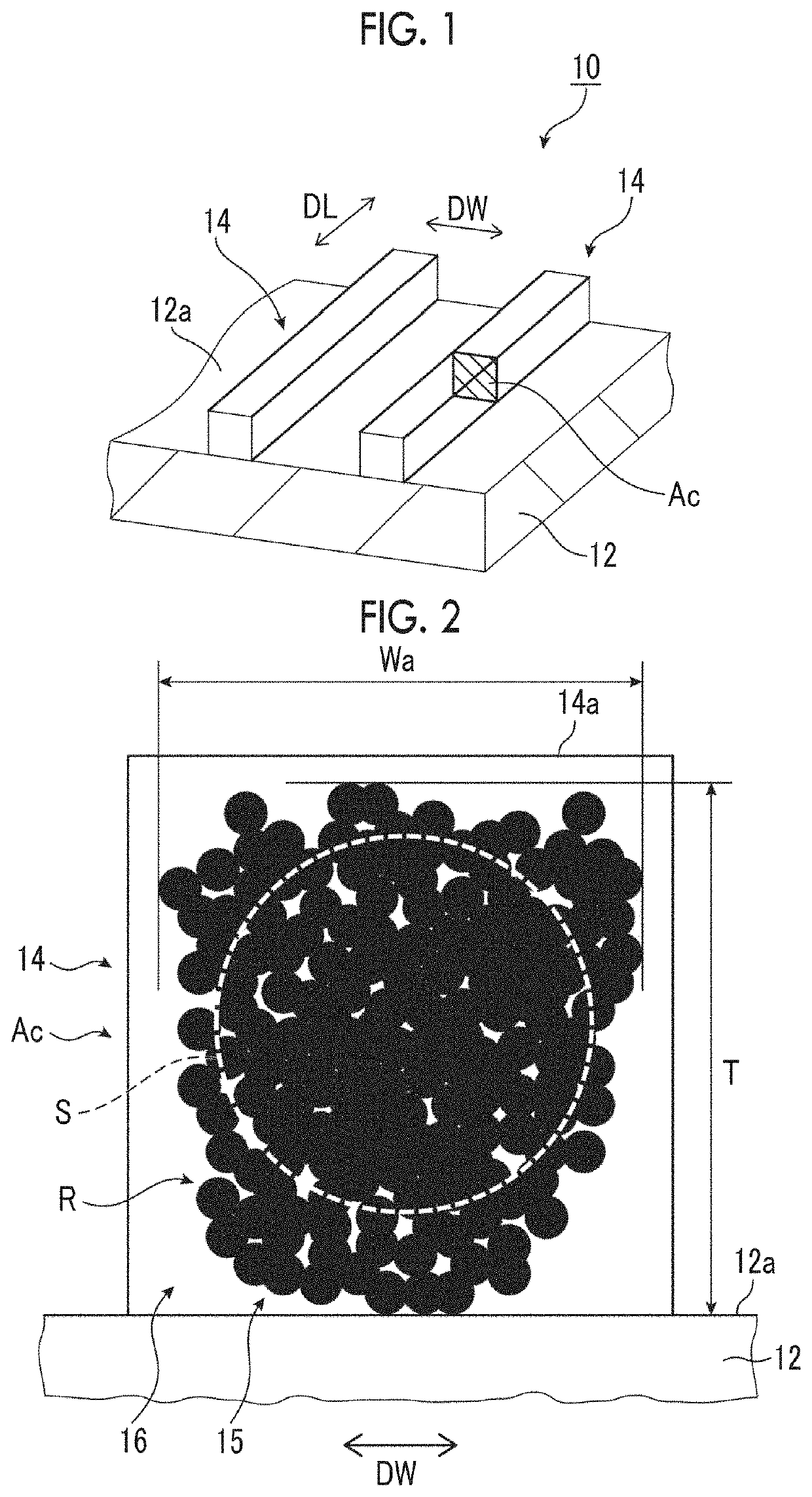
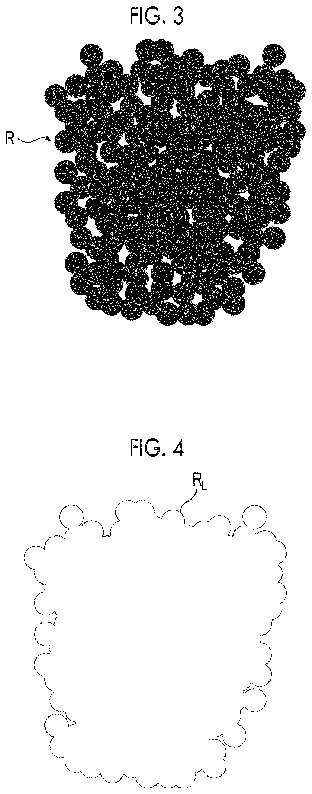
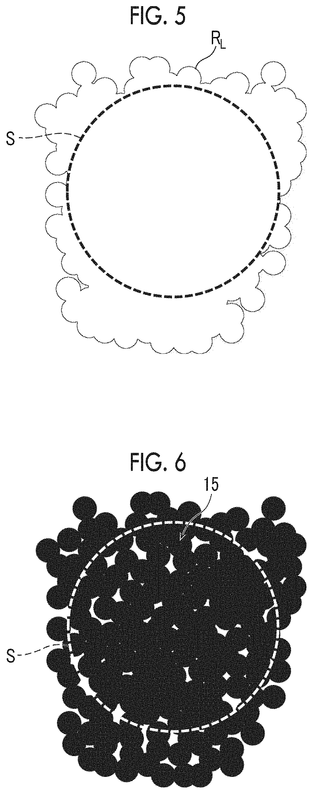
Examples
example 1
[0404]Preparation of Silver Halide Emulsion
[0405]The following liquid 2 and liquid 3 were added simultaneously in amounts corresponding to 90% of an entire amount of each thereof over 20 minutes to the following liquid 1 kept at 30° C. and a pH of 4.5 while stifling the liquid 1, whereby nuclear particles having a size of 0.16 μm were formed. Subsequently, the following liquid 4 and liquid 5 were added over 8 minutes to the obtained solution, and the remaining 10% amount of each of the following liquid 2 and liquid 3 was further added over 2 minutes, whereby the nuclear particles grew to a size of 0.10 μm. Further, 0.15 g of potassium iodide was added to the obtained solution, which was subsequently aged for 5 minutes to complete particle formation.
[0406]Liquid 1:
Water750mlGelatin8.6gPotassium bromide3gl,3-dimethylimidazolidine-2-thione20mgSodium benzenethiosulfonate10mgCitric acid0.7g
[0407]Liquid 2:
Water300mlSilver nitrate150g
[0408]Liquid 3:
Water300mlSodium chloride38gPotassium bro...
examples 2 to 12 and 18 to 22
[0446]Conductive substrates were prepared according to the same procedure as in Example 1 except that the kind of the first solution used, the temperature of the first solution used, the kind of substrate used, the line width of the conductive thin wire used, and the aspect ratio of the conductive thin wire used were changed as shown in Table 1 described later.
[0447]The line width of the conductive thin wire was controlled by adjusting the exposure amount in the step B-1. Further, the aspect ratio of the conductive thin wire was controlled by adjusting the coating amount of the composition for forming a photosensitive layer.
example 13
[0448]A conductive substrate was produced according to the same procedure as in Example 1 except that the following step 5-13 was carried out between the step D-1 and the step 2-1.
[0449]Step 5-13
[0450]The sample A obtained in the step D-1 was immersed in a 0.1% by mass aqueous laurylpyridinium chloride solution (30° C.) for 2 minutes. The sample A was taken out from the aqueous laurylpyridinium chloride solution, and the sample. A was immersed and washed in water at 30° C. for 5 seconds. Laurylpyridinium chloride manufactured by FUJIFILM Wako Pure Chemical Corporation was used.
PUM
| Property | Measurement | Unit |
|---|---|---|
| temperature | aaaaa | aaaaa |
| time | aaaaa | aaaaa |
| pH | aaaaa | aaaaa |
Abstract
Description
Claims
Application Information