Gunn diode and method of manufacturing the same

a technology of diodes and diodes, which is applied in the direction of bulk negative resistance effect devices, electrical equipment, semiconductor devices, etc., can solve the problems of rapid current change and fast current decay

Pending Publication Date: 2022-10-27
TECH UNIV DARMSTADT
View PDF0 Cites 0 Cited by
  • Summary
  • Abstract
  • Description
  • Claims
  • Application Information

AI Technical Summary

Benefits of technology

[0009]In conventional GaAs switches, the electrons in the conduction band are generated from the valence band or so-called “deep levels” between the valence and conduction bands. In contrast, the gallium nitride GaN diodes according to embodiments transfer electrons from the main valley in the conduction band to a satellite valley, which is again in the conduction band. Due to the use of GaN materials, the electron masses in the satellite valley are very high and cause a significant increase in resistance. This leads to a fast current decay. Moreover, this transfer can occur in a very short time (e.g., below picoseconds) and therefore leads to rapid current changes. Therefore, high power THz radiation can be generated.
[0010]The side contact has the effect that the field strength at the side contact is greater than in other areas, for example. Therefore, the Gunn effect is mainly effective in the side region above a certain depth, i.e. where the field strength is sufficient for electron transfer. A parasitic current that does not contribute to the Gunn effect and flows through the active layer in an inner region, within the contour of the side region, does not further disturb this Gunn effect.
[0039]Side contacting according to embodiments increases stability and also enables generation of broadband THz radiation (in the range between 50 GHz to several THz, e.g., up to 5 THz or 10 THz or even more).
[0044]Furthermore, according to embodiment examples, the new gallium nitride tunnel diode has the advantage over gallium arsenide switches that the much larger current changes can be switched stably and quickly. Since the output power is proportional to the square of the current change (P ≃ΔI2), the desired high output powers can be achieved.

Problems solved by technology

This leads to a fast current decay.
Moreover, this transfer can occur in a very short time (e.g., below picoseconds) and therefore leads to rapid current changes.

Method used


Image

  • Gunn diode and method of manufacturing the same
  • Gunn diode and method of manufacturing the same
  • Gunn diode and method of manufacturing the same

Examples


Embodiment Construction

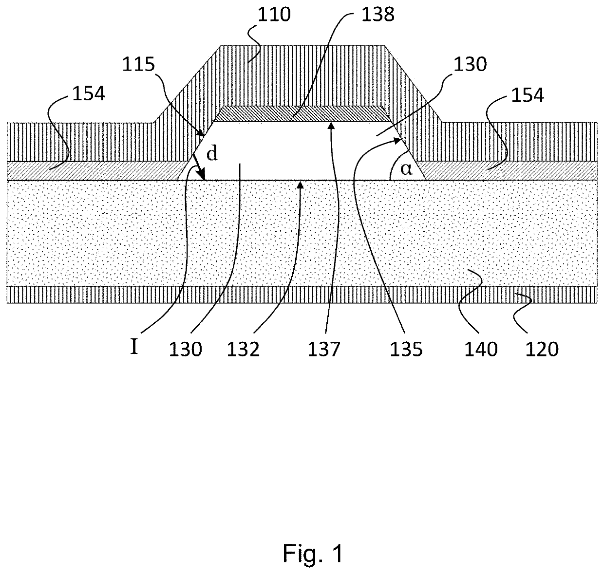
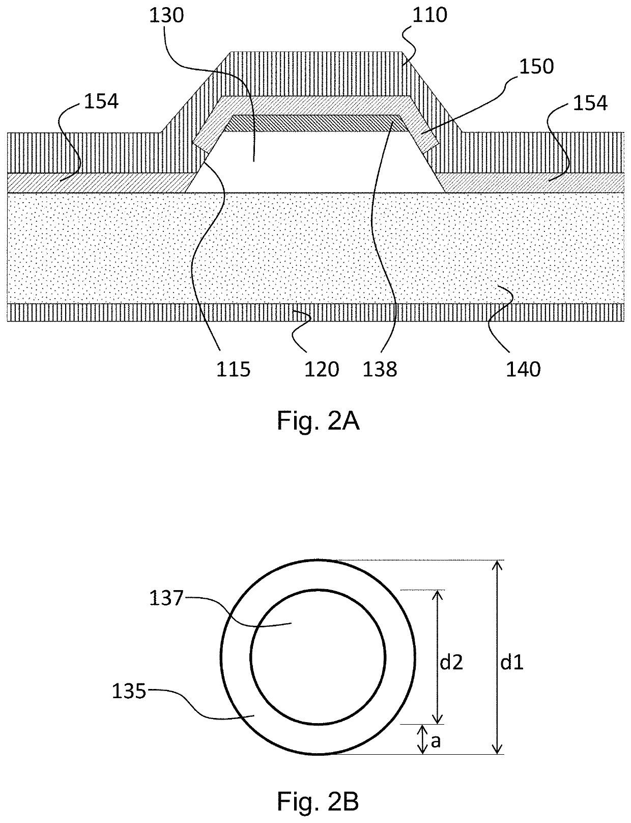
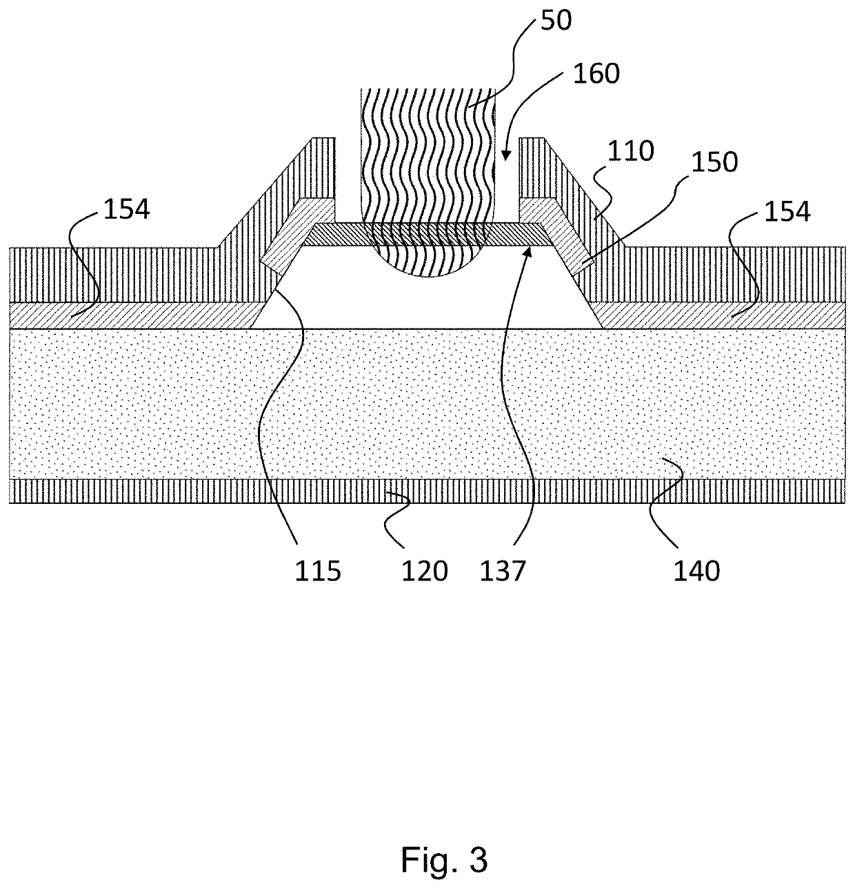
[0050]FIG. 1 shows an example embodiment of the Gunn diode. The Gunn diode includes an active layer 130 formed between a first contact layer 110 and a substrate 140, which is contacted on a back surface by the second contact layer 120. The active layer 130 is disposed on the substrate 140 with a base surface 132, and opposite the base surface 132, the active layer 130 forms a front surface 137. The front surface 137 and the base surface 132 are connected by the side surface 135.

[0051]The side surface 135 may extend completely around the active layer 130, with the first contact layer 110 electrically contacting the side surface 135 to form the side contact 115.

[0052]Along the front surface 137, the active layer 130 includes a conductive region 138 that may be formed, for example, by a highly doped region of the active layer 130, wherein the doping may be selected to adjust a desired conductivity. The purpose is to facilitate electrical contacting.

[0053]In the embodiment example shown...


PUM

PropertyMeasurementUnit
thicknessaaaaaaaaaa
thicknessaaaaaaaaaa
thicknessaaaaaaaaaa

Abstract

A Gunn diode is disclosed which comprises a first contact layer (110), a second contact layer (120), and an active layer (130) based on a gallium nitride (GaN) semiconductor material having a base surface (132) and a side surface (135) non-parallel thereto. Optionally, related materials such as aluminum indium gallium nitride (AlInGaN) materials may also be used as the active layer. The first contact layer (110) electrically contacts the side surface (135) to form a side contact (115). The second contact layer (120) forms an electrical contact for the base surface (132), so that a maximum of the electric field strength is formed when an electric voltage is applied between the first contact layer (110) and the second contact layer (120) at the side contact (115).

Description

[0001]The present invention relates to a Gunn diode and a method of manufacturing a Gunn diode and, more particularly, to a Gallium Nitride-based Gunn diode with high output powers in the high frequency range for active imaging scanners.BACKGROUND[0002]The Gunn effect has been successfully used in GaAs or InP-based semiconductor devices to generate high-frequency signals. These semiconductor materials exhibit material properties such as energy band responses, charge carrier velocities and mobilities that can initiate the electron transfer of the Gunn effect.[0003]Gunn diodes use this effect by causing electrons to accumulate and travel through the diode in bursts (like waves) through suitable circuitry (e.g. by applying an appropriate supply voltage). This in turn results in the generation and subsequent radiation of electromagnetic waves corresponding to this frequency.[0004]Especially for very high frequencies (e.g. in the terahertz range), known GaAs-based semiconductor devices h...

Claims


Application Information

Patent Timeline
Patent Type & Authority Applications(United States)
IPC IPC(8): H01L47/02H01L47/00
CPCH01L47/026H01L47/005H01L29/2003H01L33/0062H01L33/0075H01L33/385H10N80/107H10N80/01
Inventor YILMAZOGLU, OKTAYHAJO, AHID S.
Owner TECH UNIV DARMSTADT
Why Eureka
Try Eureka