

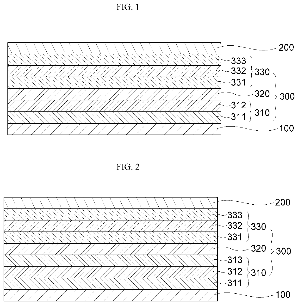
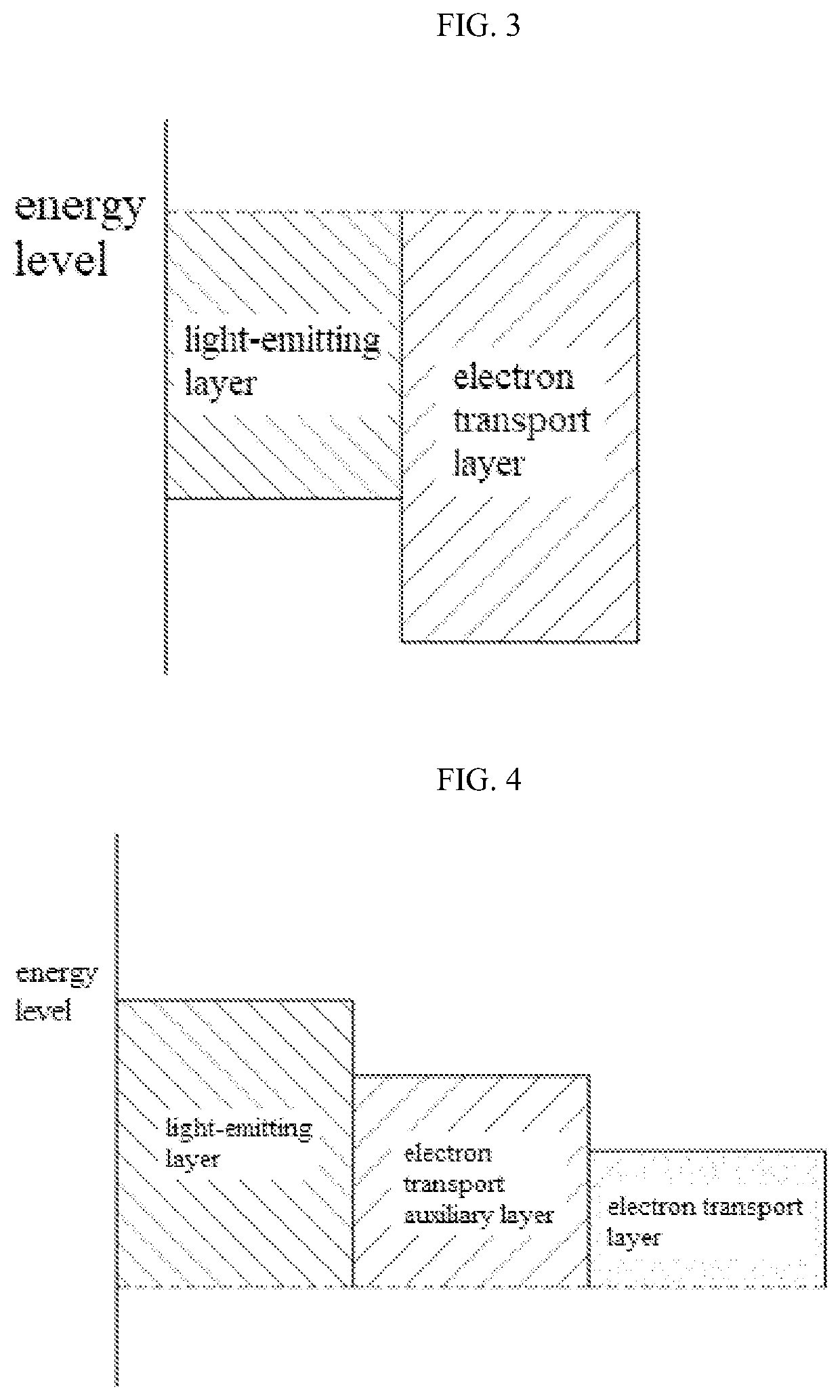
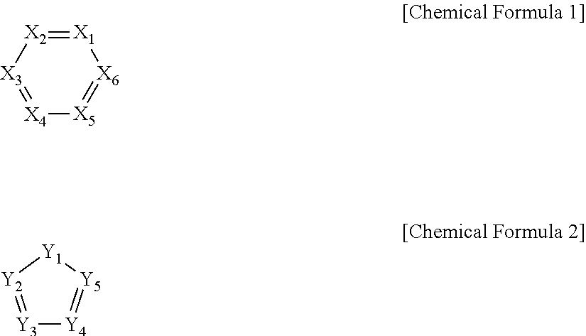
Organic electroluminescent device
a technology of electroluminescent devices and organic el, which is applied in the direction of luminescent compositions, organic semiconductor devices, luminescent compositions, etc., can solve the problems of organic el devices that have not been commercialized, the light-emitting area of organic el devices may decrease, and the light-emitting area decreases, etc., to achieve low driving voltage, high luminous efficiency, and long life
- Summary
- Abstract
- Description
- Claims
- Application Information
AI Technical Summary
Benefits of technology
Problems solved by technology
Method used
Image

Examples
embodiment 1
[Embodiment 1]—Manufacturing of Blue Organic EL Device
[0177]After high-purity sublimation purification of Compound 1 prepared in Preparation Example 1 by a commonly known method, a blue organic EL device was prepared according to the following procedure.
[0178]First, a glass substrate that had been thin-film-coated with indium tin oxide (ITO) to a thickness of 1500 Å was washed ultrasonically with distilled water. After washing with distilled water was completed, the glass substrate was ultrasonically cleaned with a solvent, such as isopropyl alcohol, acetone and methanol, dried, transferred to a UV OZONE cleaner (Power sonic 405, Hwasin Tech), and cleaned for 5 minutes using UV, and then, the glass substrate was transferred to a vacuum evaporator.
[0179]On the ITO transparent electrode prepared as above, DS-205 (Doosan Corporation Electro-Materials) (80 nm) / NPB (15 nm) / Compound 1+ADN+5% DS-405 (Doosan Corporation Electro-Materials) (30 nm) / Compound 1 (5 nm) / Alq3 (25 nm) / LiF (1 nm) / Al...
embodiments 2-14
[Embodiments 2-14]—Manufacturing of Blue Organic EL Device
[0180]Blue organic EL devices of Embodiments 2 to 14 were manufactured in the same manner as in Embodiment 1, except that each compound (‘A’) shown in Table 2 was used instead of Compound 1 which is the first host used in the formation of the light-emitting layer of Embodiment 1, and that each compound (‘C’) shown in Table 2 was used instead of Compound 1 used in the formation of the electron transport auxiliary layer.
[Comparative Example 1]—Manufacturing of Blue Organic EL Device
[0181]A blue organic EL device was prepared in the same manner as in Embodiment 1, except that Compound 1 which is the first host was not used, and that only ADN which was the second host was used in the formation of the light-emitting layer of Embodiment 1.
[Comparative Example 2]—Manufacturing of Blue Organic EL Device
[0182]A blue organic EL device was manufactured in the same manner as in Embodiment 1, except that only Compound 1 which is the first...
PUM
| Property | Measurement | Unit |
|---|---|---|
| HOMO energy level | aaaaa | aaaaa |
| LUMO energy level | aaaaa | aaaaa |
| internal quantum efficiency | aaaaa | aaaaa |
Abstract
Description
Claims
Application Information