Slotted printed circuit board surface mount stress relief system

a printed circuit board and stress relief technology, applied in the direction of printed circuit non-printed electric components association, sustainable manufacturing/processing, final product manufacturing, etc., can solve the problems of difficult solder joint thermal mismatch, high package tooling cost, and difficult thermal mismatch, etc., to reduce stress

Inactive Publication Date: 2000-01-04
SAWTEK
View PDF23 Cites 33 Cited by
  • Summary
  • Abstract
  • Description
  • Claims
  • Application Information

AI Technical Summary

Benefits of technology

In view of the foregoing background, it is therefore an object of the present invention to provide a system and a...

Problems solved by technology

For the electronic equipment manufacturer, surface mount technology carries with it a difficult solder joint thermal mismatch problem between the component or surface mount package and the PC board.
The thermal mismatch problems are especially acute for low frequency and narrow bandwidth SAW devices where the package size can be relatively large.
These problems often rule out off-the-shelf options and therefore confront the SAW manufacturer with high package tooling costs.
The solder joint is usually the weakest of the three and as a result breakage occurs in the joints at various stress points depending on the specific alloy being used.
One factor that complicates the identification of over stressed joints is that the joints are most likely to degrade but not completely fail.
In other words, they may remain electrically active for some period of time and then experience failure.
While the first cool down period after reflow begins the process of mechanically degrading the solder joint, the joints are most likely to fail after some number of thermal cycles during the normal life environment.
Another situation includes the intermittent electrical failure of the solder joint.
Such failures are difficult to detect and require more extensive testing including greater attention to the temperature cycles used and continuo...

Method used


Image

  • Slotted printed circuit board surface mount stress relief system
  • Slotted printed circuit board surface mount stress relief system
  • Slotted printed circuit board surface mount stress relief system

Examples


Embodiment Construction

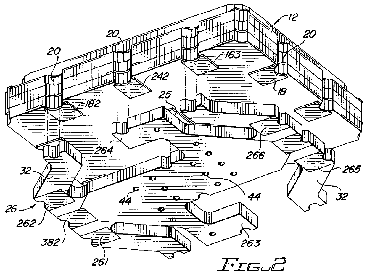
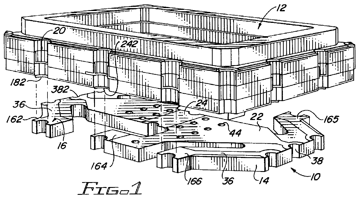
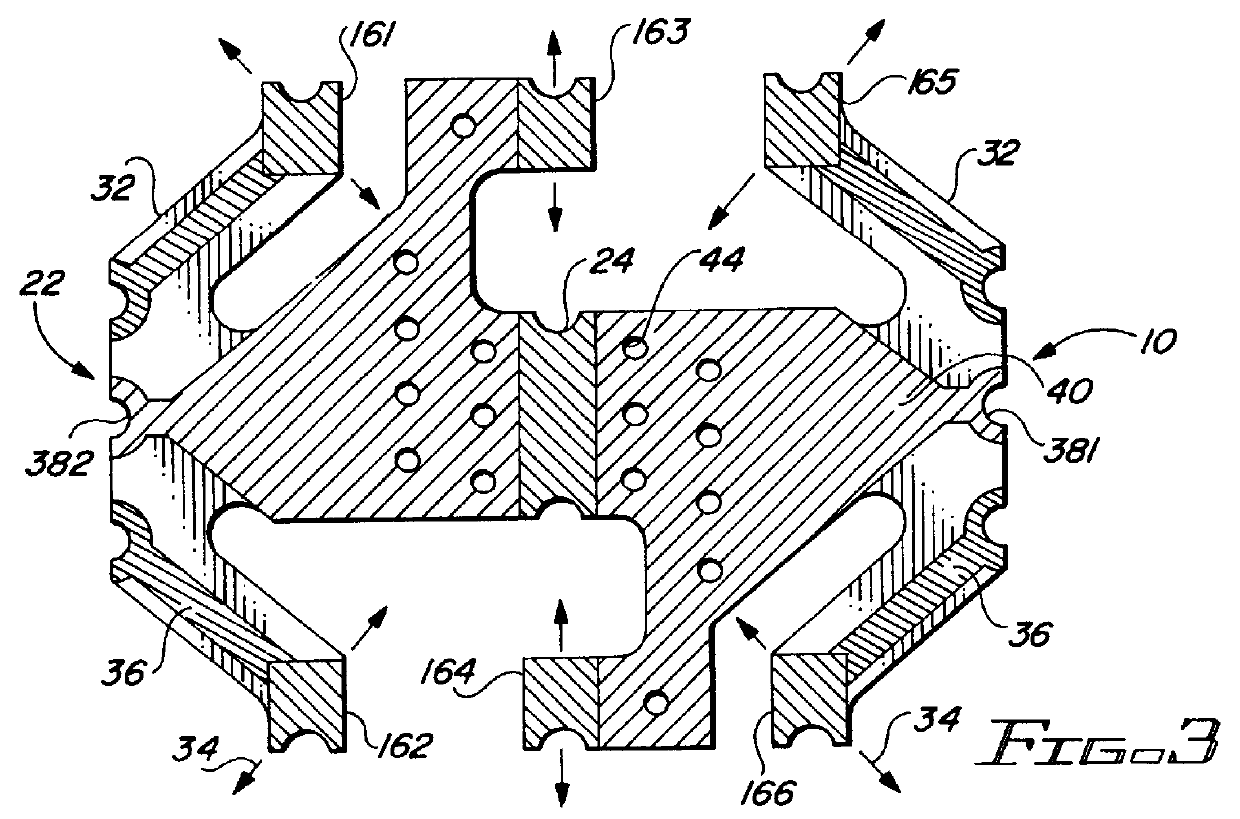
A preferred embodiment of the stress relief interface PC board 10 is shown by way of example for use with a surface mount package 12 in FIG. 1. The preferred embodiment of the device 10 comprises a PC board base structure 14 made from FR-4 epoxy and glass laminate. Other relatively compliant PC board materials well known in the art can also be used. The interface board 10 is configured to be placed between a surface mount package 12 and a printed circuit board (not shown).

In the preferred embodiment illustrated here by way of example, interface PC board 10 includes electrical contact or solder pads 16 which are sized and positioned to fit the footprint of the SMP solder pads 18. As illustrated in FIG. 2, a perspective view of the stress relief interface printed circuit board 10 in an exploded arrangement is shown with a perspective view of the surface mount package 12. The angle of view is such that the surface of the board 10 for interfacing with a printed circuit board is shown. T...


PUM

PropertyMeasurementUnit
Temperatureaaaaaaaaaa

Abstract

A surface mounting stress relief system for mounting a surface mount package such as a leadless ceramic chip carrier on a printed circuit board includes a printed circuit board having a top layer attached to a bottom layer. The top layer includes cavities for exposing top surface portion of the bottom layer which carry a plurality of solder pads. The surface mount package is positioned on the printed circuit board for placing the package bottom surface on a top surface of the printed circuit board between the cavities while positioning package contact pads in spaced relation above corresponding preselected solder pads. A solder column extends between each of the plurality of corresponding solder pads and the selected contact pads for providing an electrical connection. The solder column is formed by applying a solder paste to the solder pads on the printed circuit board, screening a low temperature solder paste onto each of the contact pads of the surface mount package, placing a solder ball onto each pad, and attaching the solder ball to each of the contact pads of the package by passing the package through a reflow oven for reflowing the low temperature solder paste without reflowing the high temperature solder ball.

Description

1. FIELD OF THE INVENTIONThis invention relates to surface mount technology using leadless integrated electronic circuit components and in particular to systems and methods for minimizing stress between the leadless component such as a surface mount package and the printed circuit board.2. DESCRIPTION OF BACKGROUND ARTSurface mount technology offers several advantages for electronic equipment manufacturers including the critical advantage of increased component packing density. One of the biggest demands for surface mount technology in the surface acoustic wave (SAW) device industry comes from the cellular and cordless telephone market. The "cigarette pack" is being replaced by the "telephone pack". For the electronic equipment manufacturer, surface mount technology carries with it a difficult solder joint thermal mismatch problem between the component or surface mount package and the PC board. The thermal mismatch problems are especially acute for low frequency and narrow bandwidth...

Claims


Application Information

Patent Timeline
IPC IPC(8): H05K1/02H05K3/34H05K3/36H05K3/28H05K1/14H05K3/30
CPCH05K1/0243H05K1/141H05K3/303H05K3/3426H05K3/3436H05K3/3442H05K3/3447H05K3/3452Y10T29/4913H05K2201/049H05K2201/09063H05K2201/09081H05K2201/09181H05K2201/0989H05K2201/09909H05K2201/10083H05K2201/10303H05K2201/10318H05K2201/10727H05K2201/10734H05K2201/10757H05K2201/10848H05K2201/10871H05K2201/10946H05K2201/10969H05K2201/10984H05K2203/041H01L2224/16H01L2924/01079H01L2924/3025H05K1/0271H05K3/28H01L2924/01087H05K2201/2036Y10T29/49144Y10T29/49139H05K3/368Y02P70/50
Inventor GORE, JOHN G.
Owner SAWTEK
Why Eureka
Try Eureka