Apparatus and methods for testing a microprocessor chip using dedicated scan strings

a microprocessor chip and scan string technology, applied in computing, measurement devices, instruments, etc., can solve the problems of chip voltage dropping below a threshold level, storage elements and dynamic circuits in the chip can lose their storage states, and the current spike is higher than averag

Inactive Publication Date: 2000-02-22
GOOGLE LLC
View PDF14 Cites 116 Cited by
  • Summary
  • Abstract
  • Description
  • Claims
  • Application Information

AI Technical Summary

Problems solved by technology

All of this leads to a higher than average current spikes in the chip, especially when the first scan clock is going active immediately after the chip has been in the idle state (clocks off).
In some cases, the inability of the power supply to compensate for the sudden drop in voltage within an appropriate time window, can lead to the chip voltage dropping below a threshold level beyond which the storage elements and dynamic circuits in the chip can lose their storage states.
Another problem encountered is storing test data received by a test or service processor from the chip under test.
The time to access the state

Method used


Image

  • Apparatus and methods for testing a microprocessor chip using dedicated scan strings
  • Apparatus and methods for testing a microprocessor chip using dedicated scan strings
  • Apparatus and methods for testing a microprocessor chip using dedicated scan strings

Examples


Embodiment Construction

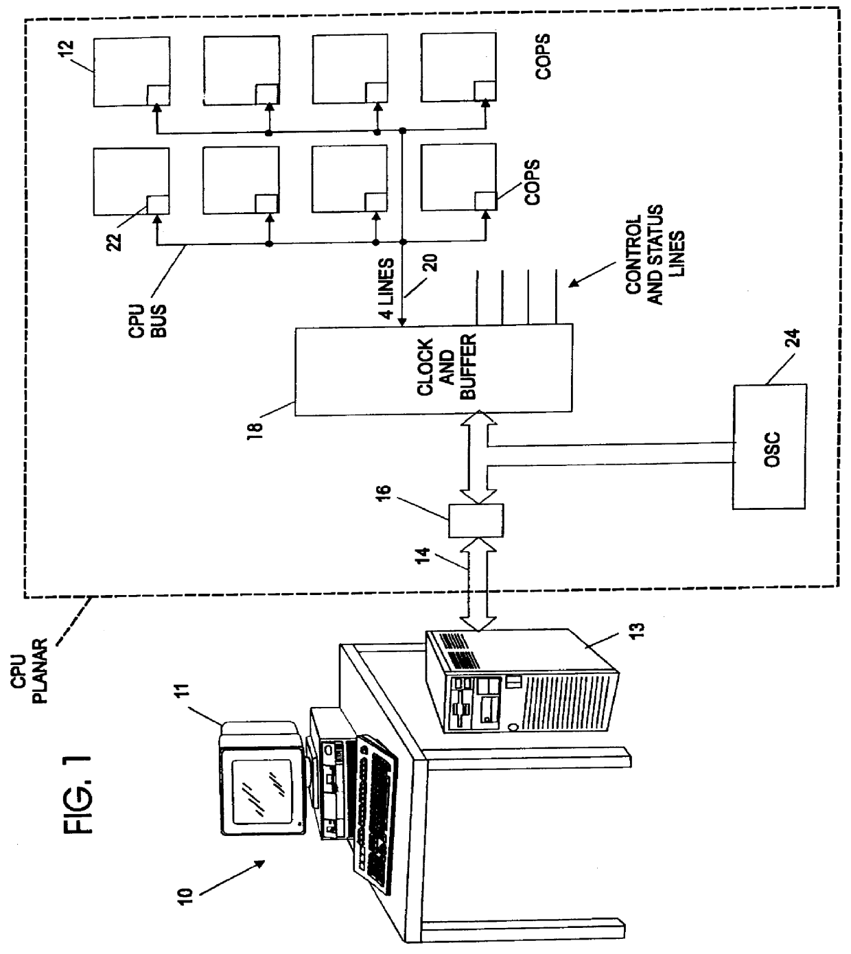
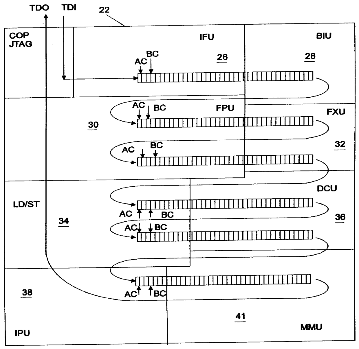
In FIG. 1, a test system 10 is coupled to a plurality of microprocessor chips 12 through a cable 14; connector 16; buffer 18 and a JTAG bus 20. Each chip 12 includes a compatible JTAG port 22 for receiving a scan train for verifying the logical design of the chip or performing a boundary scan test. The test system 12 includes a workstation 11 capable of running large programs from a permanent storage 13. The test system 10 can issue 3 classes of commands: debug, system and test. Debug commands are used only during engineering bring-up and require diagnostic programs to be executed and large data files to be manipulated, for example a dump of all system chip register latches (SRLs). System commands are part of the normal system set-up, for example, system initialization or parity error handling. Test commands control DC chip-to-chip wiring tests and stand-alone chip AC / DC self-tests for both logic and embedded arrays. An On Chip Sequencer (OCS) 24 is an off-the-shelf micro controller...


PUM


Abstract

A test apparatus and method for design verification of at least one microprocessor chip includes a compatible Joint Task Action Group (JTAG) terminal for access to a plurality of computer functional units contained in the chip. A test input terminal included in the JTAG terminal receives a scan string, the string being coupled to each computer functional unit through a first multiplexer. The scan input string is separated by the JTAG terminal under program control into a series of dedicated scan strings, each dedicated scan string being supplied to a selected functional unit through the first multiplexer. Each functional unit includes start and stop scan clocks for testing the functional under program control using the dedicated scan train for the functional unit. A test output terminal included in the JTAG terminal is coupled to each functional unit through a second multiplexer. The test results of the dedicated scan string under control of the scan clock are supplied to the output terminal through the second multiplexer. The compatible JTAG terminal includes further elements for controlling the scan clocks to select a targeted functional unit for testing purposes while the scan strings for non-targeted functional units remain in an inactive state.

Description

BACKGROUND OF INVENTION1. Field of the InventionThis invention relates to testing apparatus and methods of operation. More particularly, the invention relates to apparatus and methods for testing microprocessor chips using scan strings.2. Description of Prior ArtTesting operations for microprocessor chips usually require the chip to go from a perfectly idle state, where all the clocks, both functional and scanned are completely off, to a state where the scanned clocks are turned on for scanning. This is normally what happens every time a test or service processor is to read or write the state of the chip internal logic. Since the scan clocks affect every scannable latch element on a chip (and in some cases every dynamic circuit if the scan clock is also shared as a system clock), the node toggle activity of the chip can easily reach the 50 percent mark where, in that mode, a 0.5 probability exists that a typical node would toggle or switch to an active state. It is not very unusual ...

Claims


Application Information

Patent Timeline
IPC IPC(8): G01R31/3185G01R31/28G06F11/267
CPCG01R31/318536G06F11/2236
Inventor JABER, TALAL KAMEL
Owner GOOGLE LLC
Why Eureka
Try Eureka