Eureka AIR delivers breakthrough ideas for toughest innovation challenges, trusted by R&D personnel around the world.

Low voltage CMOS circuit for on/off chip drive at high voltage

a low-voltage cmos circuit and high-voltage drive technology, applied in logic circuit coupling/interface arrangement, pulse generator, pulse technique, etc., can solve the problems of gate oxide breakdown, hot electron effect, 3.3-volt chip connected to higher-voltage components

Inactive Publication Date: 2000-02-29
GOOGLE LLC
View PDF14 Cites 69 Cited by
  • Summary
  • Abstract
  • Description
  • Claims
  • Application Information

AI Technical Summary

Benefits of technology

Another object is a low voltage CMOS circuit which dynamically changes bias voltages for all devices to prevent device breakdown in providing high voltage on / off chip drive.

Problems solved by technology

Problems occur when a 3.3 volt chip is connected to higher voltage components.
These problems include gate oxide breakdown, hot electron effect, and undesirable reverse leakage.
Another problem is induced stresses causing breakdown condition for MOSFET devices in the gate to drain and the gate to source oxide breakdown voltage.
While the snapback / sustaining voltage can be controlled to some extent by using MOSFET's that are two to three times the minimum channel length, there are limits to the use of this technique.
The gate to source and gate to drain breakdown voltage limits are not alleviated by this technique.
None of the above prior art, alone or in combination, discloses or suggests a low voltage CMOS circuit and method of operation which utilizes intermediate voltages and voltage division techniques for multiple CMOS cascode chains between two power rails to provide higher voltages on or off chip whereby the bias voltages for MOS devices in the chains dynamically change to maintain drain to source, gate to drain and gate to source voltages within acceptable limits for device breakdown prevention.

Method used


Image

  • Low voltage CMOS circuit for on/off chip drive at high voltage
  • Low voltage CMOS circuit for on/off chip drive at high voltage

Examples


Embodiment Construction

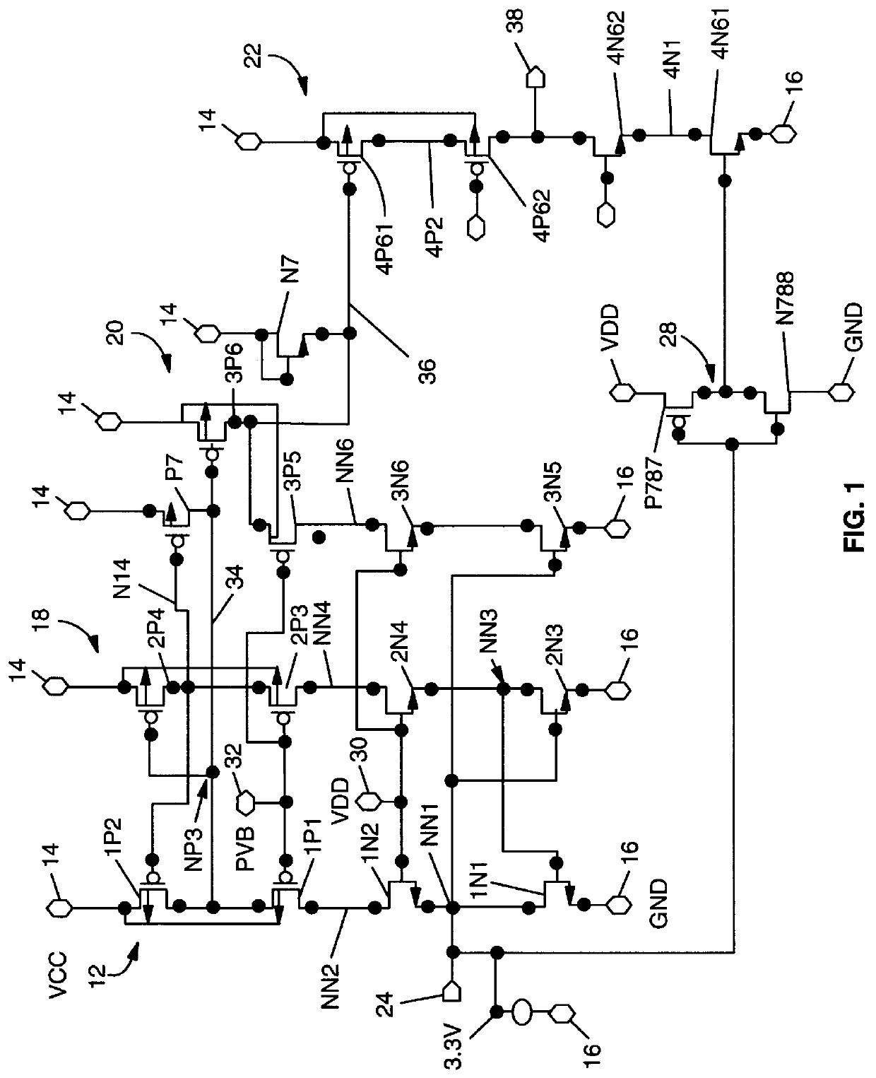
In FIG. 1, the first embodiment 10 includes a first CMOS cascode chain 12, a second CMOS cascode chain 18 and a third Cmos cascode chain 20, the chains 12, 18 and 20 being in cascade and each MOS device in the chain defined by parameters (x, y, z) where x is (1 . . . 3, the chain number; y is (N or P), the device type; and z can be (1 . . . 5) the device number in the N or P type chain. The cascode chain 12 comprises p-type MOS devices 1P1 and 1P2 in cascode and n-type MOS devices, 1N1 and 1N2 in cascode a serially connected together at a node NN2. The CMOS cascode chain 12 is connected between a high voltage power rail 14 or V.sub.cc at 5.0 volts and a low voltage power rail 16 or V.sub.ss at ground or 0 volts. The second CMOS cascode chain 18 of like configuration to cascode chain 12 is connected between the power rails 14 and 16 and consists of p-type MOS devices 2P3, 2P4 and n-type MOS devices, 2N3 and 2N4 serially connected together at a node NN4. The third CMOS cascode chain 2...


PUM


Abstract

A low voltage CMOS circuit and method provide output current ability meeting multimode requirements of high voltage off-chip drivers while protecting the CMOS devices from various breakdown mechanisms. The circuit and method utilize intermediate voltages between two power rails and voltage division techniques to limit the voltages to acceptable limits for drain-to-source, gate-to-drain, and gate-to-source of CMOS devices in any chosen technology. The circuit comprises first and second CMOS cascode chains connected between a high voltage power rail, e.g 5 volt and a reference potential power rail, e.g. ground. Each CMOS cascode chain comprises first and second p-type MOS devices in series with first and second n-type MOS devices. An input circuit is coupled to a node at the midpoint of the first CMOS cascode chain. A bias voltage, typically 3.3 volts is connected to the NMOS devices in the first and CMOS cascode chains. A second bias voltage is coupled to the PMOS devices in the first and second CMOS cascode chains. An output is provided from the second CMOS cascode chain to a third CMOS cascode chain for purposes of providing sufficient pullup capability to drive an output circuit comprising a fourth CMOS cascode chain between the high and reference potentials without exceeding the breakdown mechanisms for any MOS device in the CMOS cascode chains.

Description

1. Field of the InventionThis invention relates to semiconductor circuits. More particularly, the invention relates to low voltage CMOS circuits for on / off chip high voltage drive.2. Description of Prior ArtOften times, low voltage CMOS circuits which operate at 3.3 volts must provide higher output voltages which operate at 5.0 volts on or off the same chip. Problems occur when a 3.3 volt chip is connected to higher voltage components. These problems include gate oxide breakdown, hot electron effect, and undesirable reverse leakage. The transistor breakdown can be manifested in at least two forms. The snapback / sustaining voltage occurs when a transistor suddenly transfers from a stable operating point at high drain to source voltage to a lower drain to source voltage at a much higher current. This condition can, under certain conditions, be catastrophic and should be avoided. Another problem is induced stresses causing breakdown condition for MOSFET devices in the gate to drain and ...

Claims


Application Information

Patent Timeline
IPC IPC(8): H03K3/356H03K17/10H03K3/00
CPCH03K3/356147H03K17/102
Inventor CRANFORD, JR., HAYDEN C.GARVIN, STACY J.STEPHENS, GEOFFREY B.
Owner GOOGLE LLC
Why Eureka
Eureka Blog
Learn More