Method for manufacturing dielectric capacitor, dielectric memory device

a dielectric memory device and capacitor technology, applied in capacitors, semiconductor devices, transistors, etc., can solve the problems of affecting the performance of the dielectric memory device, and difficult to secure the capacitor area of the memory cell, so as to reduce the leakage current

Inactive Publication Date: 2000-03-07
TEXAS INSTR INC
View PDF2 Cites 86 Cited by
  • Summary
  • Abstract
  • Description
  • Claims
  • Application Information

AI Technical Summary

Benefits of technology

As a result of having conducted examinations assiduously in order to achieve said objective, the present inventors focused their attention on the fact that leakage current is rate determined by the Schottky electron emission mechanism at the interface of said bottom electrode and dielectric film. Namely, they realized that the leakage current (electron emission) depends strongly on said ...

Problems solved by technology

However, securing the capacitor area of the memory cell is becoming difficult as the enhancement in the integration progresses in, for example, DRAM.
In a dielectric capacitor, insulation property is one important performance but it was found that in the aforementioned structure, the ...

Method used


Image

  • Method for manufacturing dielectric capacitor, dielectric memory device
  • Method for manufacturing dielectric capacitor, dielectric memory device
  • Method for manufacturing dielectric capacitor, dielectric memory device

Examples


Embodiment Construction

Below, application examples of the present invention will be explained.

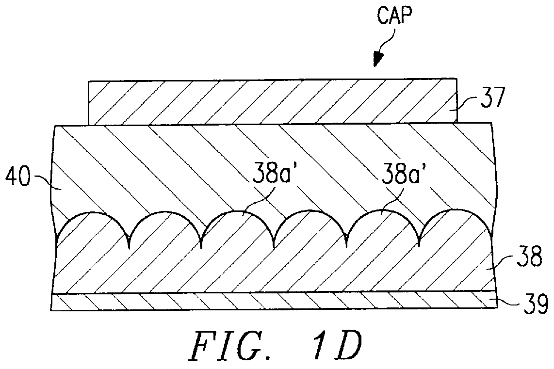
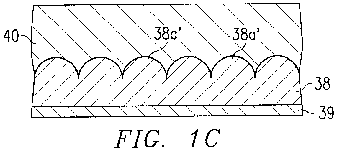
FIGS. 1A-1D are schematic sectional figures showing, with regards to the main part, an example of the process from formation of the bottom electrode to the formation of the top electrode based on the present invention.

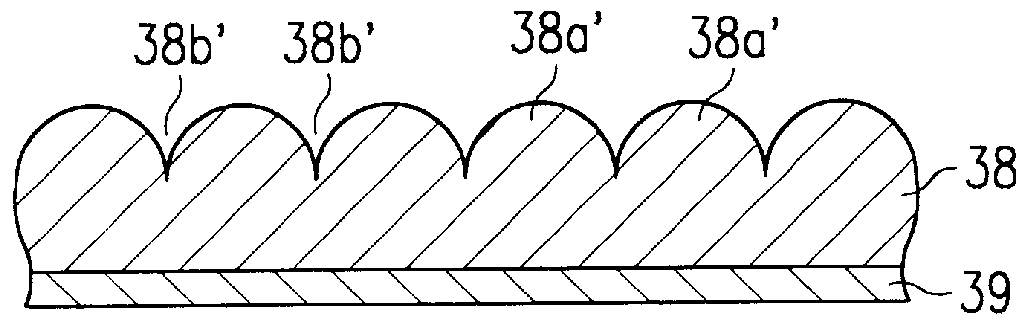
Namely, FIG. 1A shows a state of having formed bottom electrode 38 composed of Pt, etc., in a thickness of, for example, about 1000 .ANG. on barrier metal layer 39 composed of a TiN layer and a Ti adhesive layer as was noted above according to the vacuum vapor deposition method (or sputtering method), and as in what was discussed above, pointed (very small radius of curvature) convex part 38a and convex part 38b exist, for example, in a saw-toothed shape on the surface of bottom electrode 38.

Then the pointed end part of convex part 38a at the surface is polished as shown in FIG. 1B by electropolishing bottom electrode 38 in the condition to be noted later, becomes convex part 38a' flattened into a s...


PUM


Abstract

A dielectric capacitor is provided which has a reduced leakage current. The surface of a first electrode (38) of the capacitor is electropolished and a dielectric film (40) and a second electrode (37) are successively laminated on it. The convex parts pointed end (38a) existing on the surface of the first electrode is very finely polished uniformly by dissolving according to electropolishing, a spherical curved surface in which the radius of curvature has been enlarged is formed, and the surface of the first electrode is flattened. Therefore, concentration of electrolysis can be prevented during the operation at the interface of the first electrode and the dielectric film, and the leakage current can be reduced considerably.

Description

The present invention relates to a dielectric capacitor (in particular, a high-dielectric capacitor or ferroelectric capacitor) and dielectric memory device (in particular, a semiconductor memory which uses a high-dielectric capacitor or a ferroelectric capacitor), and the manufacturing method for these.Demand for high-dielectric memory devices or ferroelectric memory devices which use a high-dielectric capacitor or a ferroelectric capacitor as the semiconductor memory has been growing in recent years.A high-dielectric capacitor is that which uses a high-dielectric material such as BSTO ((Ba, Sr) TiO.sub.3) for the dielectric film and forms the cell capacitor of the memory cell in a DRAM (Dynamic Random Access Memory).Also, by using a ferroelectric material such as PZT (Pb (Zr, Ti) O.sub.3) for the dielectric film and forming a cell capacitor, a memory cell of FRAM (Ferroelectric Random Access Memory) which is a nonvolatile storage element that uses the residual polarization charact...

Claims


Application Information

Patent Timeline
IPC IPC(8): H01L21/70H01L21/02H01L21/8242H01L21/321H01G4/33H01L21/8246H01L27/10H01L27/105H01L27/108
CPCH01L27/1085H01L28/60H01L21/32115H10B12/03
Inventor AOKI, KATSUHIROFUKUDA, YUKIONUMATA, KENOKUNO, YASUTOSHINISHIMURA, AKITOSHI
Owner TEXAS INSTR INC
Why Eureka
Try Eureka