
IPO deposited with low pressure O3-TEOS for planarization in multi-poly memory technology

a memory technology and deposited layer technology, applied in the direction of semiconductor devices, electrical equipment, nanotechnology, etc., can solve the problems of uneven underlying topology, high surface sensitivity, and several problems of interpoly oxide layers formed under polysilicon load resistors

Inactive Publication Date: 2000-03-21
TAIWAN SEMICON MFG CO LTD
View PDF11 Cites 2 Cited by
  • Summary
  • Abstract
  • Description
  • Claims
  • Application Information

AI Technical Summary

Benefits of technology

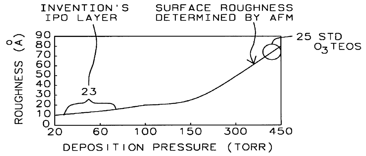
The invention's O.sub.3 -TEOS process with it's lower pressure range makes the IPO layer 11 surface smoother. The inventor theorizes that at the lower pressure that the recombination of the pre-cursor of O.sub.3 and TEOS reaction is reduced therefore creating a smoother surface.
As a comparison, the inventor's standard O.sub.3 TEOS layer has a surface roughness (measured by the AFM) is between about 80 to 100 .ANG.. This is about 400% rougher than the invention's low pressure O.sub.3 -TEOS IPO layer. It is important to note that SACVD TEOS layers are used in the industry for back end processes, but not used for IPO layers because of their high surface sensitivity. This surface sensitivity causes resistance fluctuations. Moreover, the conventional SACVD oxide changes the value of the resistors compared to resistors formed over LPTEOS IPO layers (which are commonly used). In addition, Standard SACVD layers have moisture absorption problems that are eliminated with the invention's process.

Problems solved by technology

The inventor has found that current inter-poly oxide (IPO) layers that are formed under polysilicon load resistors have several problems.
First, a problem with current dielectric layers (IPO) under resistors is that the underlying topology is very rugged and uneven.

Method used


Image

  • IPO deposited with low pressure O3-TEOS for planarization in multi-poly memory technology
  • IPO deposited with low pressure O3-TEOS for planarization in multi-poly memory technology
  • IPO deposited with low pressure O3-TEOS for planarization in multi-poly memory technology

Examples


example 2--

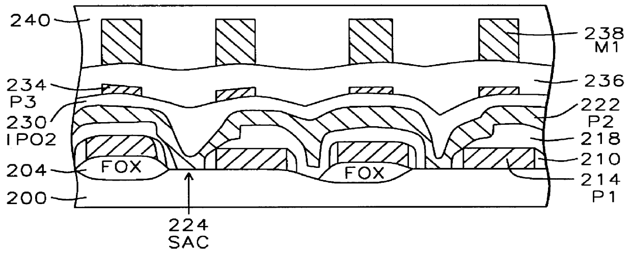
IPO-2 layer in SRAM-FIG. 5

FIG. 5 shows another example (preferred embodiment) of an SRAM having an inter-poly oxide (IPO-2) 230 that is formed using the invention's low pressure O.sub.3 -SACVD TEOS process. FIG. 5 shows a semiconductor substrate 200 having at least an isolations area 204 and an active area. Next, a first polysilicon layer 214 (P1) is deposited over the substrate surface. The first polysilicon layer is patterned to form a conductive line over the isolation region and a gate electrode over the active area. Next, insulating sidewall spacers 210 are formed on the gate electrode and conductive lines. Then doped regions (not shown) are formed adjacent to the gate electrode. The doped regions serving as source and drain regions. A first inter-poly oxide (IPO) layer 218 is formed over conductive line and the gate electrode and elsewhere over the substrate surface. The IPO layer (LPCVD TEOS oxide) can be formed by depositing silicon oxide at a temperature between 600 and 800...

example 3

of the Invention's IPO layer

Another example of a SRAM that can be formed using the invention's invention's O.sub.3 -SACVD IPO layer is shown in U.S. Pat. No. 5,652,1 74(Wuu et al) to the same assignee which is hereby incorporated by reference into this patent. In Wuu, FIG. 6, the IPO layer 30 can be formed using the invention's O.sub.3 -SACVD IPO layer. In Wuu in col. 7, line 7 to 10, Wuu teaches a conventional LPCVD TEOS IPO layer. In contrast, Wuu's layer 30 is advantageously formed using the inventor's Low pressure O.sub.3 -TEOS SACVD IPO process as described above.

Benefits of the Invention's IPO Layer

The SACVD O.sub.3 -TEOS IPO layer of the present invention controls the resistivity of the overlying polysilicon resistor by making the surface of the IPO layer smoother and more planar. The invention's smoother IPO surface makes the load resistor resistance (load.sub.-- RS) more uniform. In a SRAM cell, there are two poly--load resistors. Generally, these two polysilicon resistors ...


PUM


Abstract

The present invention provides a method of inter-poly oxide (IPO) layer underlying a polysilicon resistor in a memory product. The IPO layer 15 is formed by a modified low pressure SACVD-O3-TEOS process that gives the IPO layer a smoother surface and good planarization. This IPO layer gives the overlying polysilicon resistors a more uniform resistance. The method begins by providing a semiconductor structure 10. Next, in an important step, an inter-poly oxide (IPO) layer 11 is formed using low pressure ozone assisted sub-atmospheric chemical vapor deposition (SACVD O3-TEOS) process at a pressure between about 20 and 150 torr. A polysilicon resistor 15 is then formed on said inter-poly oxide (IPO) layer. The memory device is completed by forming passivation and conductive layers thereover.

Description

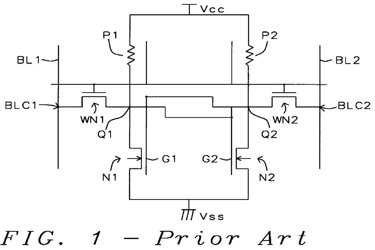
1) FIELD OF THE INVENTIONThis invention relates generally to the fabrication of a dielectric layer and a resistor for a semiconductor device and more preferably a method for forming an inter-poly oxide (IPO) layer using a O.sub.3 -SACVD process under a polysilicon resistor for a memory device.2) DESCRIPTION OF THE PRIOR ARTInter-poly oxide (IPO) layer planarization is a critical process in semiconductor manufacturing and more particularly in memory devices, especially SRAM products. The rough topology of underlying devices reduces photo depth of focus (DOF) and induces etch residues.A circuit schematic for a typical polysilicon load resistor SRAM cell, commonly referred to as poly-load SRAM is shown in FIG. 1. Only one of the cells in the array of cell is shown in FIG. 1. The SRAM circuit is fabricated using polysilicon resistors that are doped with an N-type conductive dopant of the load resistors, labeled P1 and P2 in FIG. 1. Two N-channel FETs formed in and on the substrate are u...

Claims


Application Information

Patent Timeline
Patent Type & Authority Patents(United States)
IPC IPC(8): H01L21/70H01L21/8244H10B10/00
CPCB82Y15/00H01L27/11H10B10/00
Inventor WUU, SHOU-GWOCHEN, LUNGYAUNG, DUN-NIANLIN, YI-MIAW
Owner TAIWAN SEMICON MFG CO LTD
Learn More